What is the Cutoff of a Waveguide?
March 22, 2023A waveguide is a medium for the transport of RF signals. The medium can support many Transverse Electric (TE) or Transverse Magnetic (TM) modes. Normally, only the lowest order mode between the cutoff and the beginning of the next higher order mode is used, which is TE10 or TM11. Using a waveguide at a frequency where more than one mode is possible is not advised, as different modes have different group velocities.
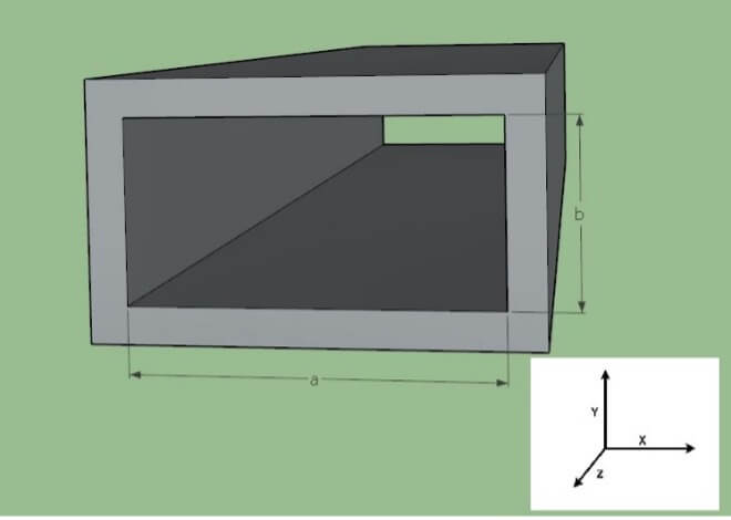
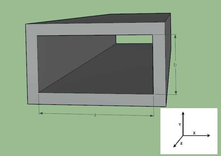
The low frequency cutoff of a rectangular waveguide for mode TEmn in terms of dimensions a and b is given by:![]()
The formula is the same for TM modes, but TM10 is not realizable. The first transverse magnetic mode is TM11.
The component of the wave vector in the z-axis direction of propagation is given by:

And the phase velocity is:![]()
And group velocity is:
For example, a WR-112 waveguide has dimensions, a = 2.85 cm and b = 1.26 cm. For TE10 mode, Fc is simply c/2a or 5.26 GHz.
The insertion loss of the WR-112 waveguide is shown below in Figure 1:

Figure 1 -WR-112 Waveguide Response Showing Cutoff
Typically, this waveguide is used from 7.05 to 10 GHz.
See this and more important radio frequency charts and formulas in this comprehensive application note.
Related Post

What Are the VNA Display Formats and What Do They Mean?
August 10, 2023
Introduction Fundamentally, a Vector Network Analyzer (VNA) measures RF reflections. In a 50Ω system, reflections occur whenever an impedance other than 50 ohms is encountered by the RF signal. The reflection has a magnitude and a phase with respect to the magnitude and phase of the incident signal and may be characterized as a complex number. The VNA menu allows for a selection of charts which can display complex reflection coefficients in many different ways. Read on to learn more about VNA display formats available for analyzing measurements. Reflection and Reflection Coefficients In optics, if a beam of light traveling in a media with dielectric constant ε1 encounters a region with dielectric constant ε2, there will be a reflection as shown in Figure 1. Figure 1 - Optical Reflection The magnitude of the reflection is related to the difference between the two dielectric constants. The transmitted and reflected waves may be normalized by dividing by the incident wave to arrive at a Reflection Coefficient, Γ. For instance, in the absence of loss, the coefficient for reflection might be 0.2, thus the coefficient for transmission must be 0.8. Here, the reflection coefficient is ratio-metric, and the magnitude of the incident signal is irrelevant. Similarly, an RF voltage wave travelling on a 50Ω transmission line may encounter an impedance other than 50 ohms. This results in a reflection. Specifically, that reflection is given by: Where Z is the encountered impedance. If Z is a complex impedance –which can be expressed as R+jX– such as a resistor and capacitor in series, the reflection coefficient Γ will also be complex. We can choose to display the complex reflection coefficient in the following ways: VNA Display Formats Log Magnitude In this format, the magnitude of the complex reflection coefficient is calculated, the base 10 logarithm is applied, and the result multiplied by 20. The multiplication by 20 makes the result proportional to power instead of voltage. Where the complex reflection coefficient Γ is a+jb. This format is convenient to examine a reflection coefficient over a very wide dynamic range. Details of the low loss in the passband of a filter along with a very deep stopband can be clearly seen in Figure 2. This would not be possible using a linear scale. Figure 2 - Filter Plot Linear Magnitude The linear scale is convenient to examine a transmission coefficient such as S21, where the linear magnitude covers a range within two to three orders of magnitude. Figure 3 shows the same filter from Figure 2 but in the linear scale. Details at markers 2 and 3 are not distinguishable in this format. Figure 3 - Filter in Linear Scale Delay The delay format shows the group delay, which is calculated from -dФ/dω of S21. Ф is the phase of the reflection coefficient and ω is the radian frequency, 2πf. The group delay of the filter in Figure 2 is shown below in Figure 4. Figure 4 - Filter Group Delay VNA Display Format The group delay varies from 7.2 nS to 15.4 nS in the passband of the filter. If a modulated signal were passed through this filter such that some of the modulation bandwidth extends toward the peaks, there would be significant phase distortion (dispersion). Frequencies near the peaks might arrive at the receiver 5 nS or so later than frequencies near the center. Filters can be designed with much flatter delay than this if needed, and this can be evaluated using this delay display mode. Phase The phase of the reflection coefficient can be displayed on the VNA screen. The phase is the arctangent of the ratio of the imaginary and real parts of the coefficient, but it represents the phase alignment of the reflected or transmitted signal with respect to the incident signal. If the two signals are in perfect alignment, the phase difference is zero. The phase depends greatly on the delay experienced by the signal. Figure 5 shows the phase of the signal passed through the filter of Figure 2. Figure 5 - Filter S21 Phase The phase wraps at -180 and 180 degrees. The curvature on the left and right sides is due to the delay variation shown in Figure 4, whereas the phase is reasonably linear where the delay is flat in the middle of the passband. Extended Phase The phase is not wrapped in extended phase mode. The phase will be near zero at low frequencies and then become more and more negative at higher frequencies. The phase will change at a greater rate as more delay is experienced. Figure 6 - Extended Phase Display SWR The Standing Wave Ratio is used on reflection measurements such as S11. Reflections on a transmission line interfere with the incident wave, creating peaks and valleys in the voltage envelope of the RF wave. The ratio of the peaks to the valleys along the transmission line is the SWR. An SWR of 1:1 means there are no peaks or valleys, and hence no reflection. SWR may be calculated from the linear reflection coefficient, Γ. Real and Imag The Real and Imaginary display formats depict the real or the imaginary components of a reflection coefficient. Note, these are not the real and imaginary components of an impedance. If there is no imaginary component, then the impedance contains no reactive component and must be resistive alone. If there is no real component, the impedance must be reactive alone. Polar The polar format plots the complex reflection coefficient within a unit circle with the real component on the horizontal axis and the imaginary component on the vertical axis. This is the most fundamental plot, as it displays the reflection coefficient in its most basic form. All other formats are useful derivations. A reflection coefficient is essentially a complex vector. The polar format plots the magnitude and phase of this vector. A vector is often drawn as an arrow, but a dot at what would be the tip of the vector is drawn to reduce clutter when showing vectors for many frequencies. A VNA display format of a polar chart will have circles of magnitude and radial lines of angle, as shown below in Figure 7. Magnitude is shown in linear format here. Figure 7 - Polar Plot If Polar(log) is chosen, the magnitudes of the makers will be stated in dB format. The polar Smith formats, Smith(log), Smith(Lin), Smith(Re/Im), and Smith(R+jX) are Polar plots with a Smith chart overlay. The Smith overlay maps the polar reflection coefficient to the corresponding impedance, which gives rise to it as calculated from Eq. 1. The variations above merely change the values given by the markers. Figure 8 - Smith(R+jX) Format Smith(log) will give the log magnitude and angle of the reflection. Smith(Lin) will give the linear magnitude and angle. Smith(Re/Im) will give the linear Cartesian format reflection. Smith(R+jX) will give the complex impedance at each point. Smith(G+jB) uses the admittance overlay on the polar plot. Instead of an R+jX impedance, the marker value will show the G+jB admittance, which gives rise to the reflection, where the R+jX mode gives the impedance of a pair of series components, a resistance and a reactance. The equivalent inductance or capacitance at that frequency is also given. The G+jB admittance gives the conductance (inverse of resistance) and the susceptance of two components in parallel. The Smith(R+jX) is convenient for analyzing an impedance, which is best modeled as a series impedance, while Smith(G+jB) is best for analyzing a parallel admittance. Conclusion Different display formats are useful for different measurements. This application note covers several different display formats and their uses. For example, the Log Mag format might be best for evaluating a filter, but the SWR will likely be used to evaluate the input match of an antenna, and the Smith(R+jX) is useful for measuring an impedance and perhaps working out a matching network.

Useful Radio Frequency Engineering Formulas and Charts
February 9, 2023
This application note is a collection of essential formulas and charts for Radio Frequency Engineering.

What is a Waveguide?
January 31, 2023
A waveguide is rectangular, circular, or oval “pipe” filled with air or dielectric material which is capable of conveying RF energy. The physical implementation of the structure determines the frequencies which may be transported. Many Eigenmodes are possible, but the lowest order is almost always used. Equations for the calculation of these modes for rectangular waveguides are detailed below. A chart of common commercially available waveguides is included at the document’s conclusion.

Waveguide Calibration of Copper Mountain Technologies' VNAs
April 19, 2018
Waveguide components possess certain advantages over their counterpart devices with co-axial connectors: they can handle larger power and exhibit lower loss. Therefore, it is very common to employ waveguide interfaces in the high power devices, such as microwave transmitters. The performance of waveguide components at microwave frequencies are typically measured with a Vector Network Analyzer (VNA). However, when measuring the performance of waveguide components with a VNA, non-idealities of any uncalibrated VNA introduce uncertainty in the measurement results. This application note describes how to perform an SSL calibration with a Copper Mountain Technology VNA. It also covers the procedures and the calculations to define a waveguide calibration kit in the CMT VNA. Finally, it provides an example of the 1-port return loss measurement of a waveguide band-pass filter.


