USB Vector Network Analyzers from Copper Mountain Technologies

CMT USB vector network analyzers

What is a Vector Network Analyzer (VNA)?

A USB vector network analyzer produces an RF stimulus signal which can be in the range of 9 kHz to 330 GHz. That signal can be applied to a Device Under Test (DUT) and the output of the DUT can be applied to a second port for analysis. In addition, any reflections from the input of the DUT which travel back to the source port can be analyzed as well. This is what differentiates the device from other test equipment – it is capable of separating signals traveling in two different directions on a transmission line and measuring them.

What Does a Vector Network Analyzer Do and How Does a Vector Network Analyzer Work?

Figure 1 shows a simplified block diagram for a USB vector network analyzer. The Port 1 and Port 2 bridges shown are the components which separate the forward and reverse traveling RF waves. Receivers R1 and R2 pass only a sample of the wave exiting Ports 1 or 2. Receivers A and B pass only a sample of waves entering Ports 1 or 2. Note that only three receivers are active at any time. Receiver R1 is active when the stimulus is switched to Port 1, and R2 is active when it is switched to Port 2.

When the stimulus signal is switched to Port 1, the magnitudes and phases of the signals on reflection receivers A and B are normalized to stimulus receiver R1. In this way, the absolute output power of the stimulus is irrelevant. Similarly, when the stimulus is switched to Port 2, measurements A and B are normalized to receiver R2.


The performance of a linear DUT can be predicted under any source and load impedance with knowledge of transmitted and reflected signals (S-parameters) from both sides.

VNA Block Diagram with Port 1 Reflections

Figure 1 – VNA Block Diagram with Driven Port 1 Reflections

What is the Vector Network Analyzer Working Principle?

For a full 2-port measurement, the stimulus switches back and forth between Ports 1 and 2. When at Port 1, Receiver A, R1, and B are measured. The value A/R1 will be raw S11 and B/R1 will be raw S21. The stimulus then switches to Port 2 where B, R2, and A are measured. B/R2 will be raw S22 and A/R2 will be raw S12. The normalization occurs in an FPGA after the three receiver measurements are made in each direction. Within the FPGA, the IF Bandwidth filtering is applied using DSP and the data is then heavily decimated.

The now low data-rate decimated raw data, S11, S12, S21, and S22 are sent via USB connection to the Copper Mountain Technologies (CMT) vector network analyzer software running on the host computer so that calibration can be applied, and the results are displayed in the desired format.

What is a Vector Network Analyzer Used For?

USB Vector Network Analyzers can be used for a variety of applications. For example, a VNA might be used to evaluate an amplifier used in an RF system. RF amplifiers may be characterized for gain, return loss, P1dB, output match, and stability. These characteristics are important to verify when designing an amplifier into a system.


A VNA can also be used to evaluate the properties of an RF filter. Filters are an important part of most RF systems. A receiver designed to operate over a set bandwidth will invariably have a filter on the front end to limit the input to those frequencies. If the signal is mixed up or down to another frequency, a filter is required before the mixer to prevent ambiguous mixing at the image frequency.


A VNA can measure the passband insertion loss of a filter, S21, and the return loss at the input, S11. It can also measure the stopbands and VNAs from CMT have exceptional dynamic range which allows them to measure both passband and deep stopbands in one measurement as shown in Figure 2.


An antenna may be evaluated with a VNA. An antenna should convert a signal on its feedline into radiated RF energy if the frequency is within its operating bandwidth. A reflection measurement is sufficient to evaluate the suitability and health of an antenna. If there is high reflection, then clearly there will be little energy radiated. Conversely, if the reflection back from the antenna is low, it can be assumed that energy is being radiated away. Return loss (S11) or VSWR are the usual measured parameters.

Filter Measurement with USB Vector Network Analyzer
Figure 2 – Filter Measurement

Cables and waveguides can be measured with a VNA. It is very common to use a VNA in the production of RF cables. 1-Port handheld and portable VNAs from Copper Mountain Technologies are conveniently used to verify proper cable performance while it is still on the production machine. Cable feedlines to antennas may be evaluated using the Time Domain mode to verify characteristic impedance over distance to check for damage or moisture ingress.

Waveguide transmission lines can be measured with a suitable coaxial to waveguide adapter. As an example, the long waveguide run from the radar to the transmitting antenna on a naval vessel may be evaluated using the Time Domain feature much like a cable feedline. Dents, dings, or rusted waveguide section bolts can be quickly located.

The dielectric properties of materials may be measured with a VNA. Millimeter wave VNAs may be used to perform material measurements. A sheet of a material to be measured is held in a frame between two antennas connected to a VNA as in Figure 3. Two lenses focus the beam to transform the circular wavefronts into plane waves. The dielectric properties of a sheet material may be measured in this way.

This might be important to evaluate a material used for a radome. The complex dielectric constant of the material can be calculated from over-the-air S-parameter measurements.

Vector Network Analyzer vs Spectrum Analyzer

So what is the difference between a VNA and spectrum analyzer? A USB vector network analyzer (VNA) is very different from a spectrum analyzer (SA). The former is used to measure the transmission and reflection characteristics of a Device Under Test (DUT), and the latter is suitable for measuring the amplitudes of frequencies applied to its input. Where an oscilloscope might display the time domain response of a number of input signals, an SA displays the Fourier transform of the signals, showing the distinct amplitude of each frequency component.

Figure 4 and Figure 5 show an oscilloscope and a spectrum analyzer measurement of two signals, one at 130 MHz and the other at 220 MHz.

The utility of the spectrum analyzer is clear. It distinctly shows the amplitude of the two frequency components separately, where the frequency content of the oscilloscope measurement is difficult to interpret.

There are major differences between the block diagrams of an SA and a VNA. A typical SA block diagram is shown in Figure 6. Double conversion (double heterodyne) is required to ensure that mixer images are not an issue. Additionally, the Local Oscillator (LO) sources, particularly the first one in the block diagram below, must be free of spurious signals, and high order intermodulation products (IMs) must now show up in the 15 GHz IF. An additional IF path must be switched in if IMs cannot be avoided, and the LO offset changed accordingly. In other words, a 15.15 GHz IF filter might be switched in instead of the 15 GHz filter, and the first LO would be moved up by 200 MHz for this IF path and only for frequencies where there are unavoidable spurs in the first IF frequency.

Oscilloscope Measurement of 130 and 220 MHz Signals
Figure 4 – Oscilloscope Measurement of 130 and 220 MHz Signals


Spectrum Analyzer Measurement of 130 and 220 MHz Signals

Figure 5 – Spectrum Analyzer Measurement of 130 and 220 MHz Signals


The SA is therefore considered a broadband tracking receiver and displays the amount of existing RF power at each frequency within an IF bandwidth determined by FIR filtering in the DSP section.


Spectrum Analyzer Block Diagram
Figure 6 – Spectrum Analyzer Block Diagram


Some spectrum analyzers come with a tracking generator. The generator sweeps along with the tracking receiver. With the generator attached to the input of a DUT and the output connected to the SA input, you can measure the frequency response of a DUT. This function is similar to what a VNA does, but a USB vector network analyzer would be much more precise and include phase information.

How Does the Spectrum Analyzer Design Compare to a VNA?

A VNA has a much simpler RF architecture. A stimulus signal— which steps from a start frequency to a stop frequency— passes to a DUT, and then tracking receivers measure signals which pass through and are reflected back. The receivers are only sensitive to signals at the generated stimulus frequency and only within the IF bandwidth of measurement.


A typical VNA block diagram is shown in Figure 7. The stimulus signal is routed to either Port 1 or Port 2 and passes through a directional bridge on each side. The bridges are capable of separating signals by direction of travel, so the two output ports of the bridges are a sample of the amount of signal leaving the port and the amount entering the port. A mixer on each port of each of the bridges reduces the high stimulus frequency to a much lower IF frequency, usually below 20 MHz. The constant frequency IF is digitized, and a low latency DSP filter is used to apply the IF Bandwidth (IFBW). Only a single conversion is done, not dual as in a spectrum analyzer.


A block diagram such as this is susceptible to mixer image ambiguity. For instance, if the LO is 10 MHz above the stimulus to create a 10 MHz IF, then the desired response is caused by a signal 10 MHz below the LO, but a signal 10 MHz above will also create the very same IF signal. However, that is not how a VNA operates.


There is only one signal— the stimulus— and it is completely controlled by the USB vector network analyzer and is always at LO-IF in frequency. The image is not an issue for normal VNA measurement, so a single conversion (homodyne) architecture is acceptable.


The receivers in the VNA are also tracking receivers as in an SA, and you can use a VNA as a rudimentary SA by turning off the stimulus signal and observing the signal power measured by one of the receivers— A or B — which respond to signals entering VNA ports one or two respectively.

Typical USB vector network analyzer Block Diagram
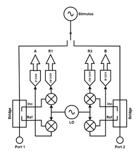
Figure 7 – Typical VNA Block Diagram

USB Vector Network Analyzer Used as a Spectrum Analyzer
Figure 8 – VNA Used as a Spectrum Analyzer


1 kHz DSP IF Bandwidth Filter

Figure 9 – 1 kHz DSP IF Bandwidth Filter

Actual SA Measurement of a Signal with 1 kHz IFBW and 100 kHz Span
Figure 10 – Actual SA Measurement of a Signal with 1 kHz IFBW and 100 kHz Span

A single signal applied to the USB vector network analyzer will show two responses— one at the actual frequency and another at the image— or twice the IF frequency lower. There may also be some small spurious signals from the LO. A VNA LO does not have to be pristine like the ones used in an SA, since the VNA normally only measures its own stimulus frequency.


Figure 8 shows a signal close to 2.3 GHz being measured by the A receiver of the VNA. The VNA stimulus source has been turned off and the absolute A receiver measurement has been chosen with a 100 kHz span around 2.3 GHz. The side lobes of the low latency VNA IF Bandwidth filter implemented in DSP are clearly visible. An SA would use a DSP with minimal sidelobes since accurate signal visualization is more important than measurement speed. The DSP IF filter in the VNA is optimized for lowest delay to reduce measurement speed. The sidelobes of the VNA IF filter do not degrade VNA measurement accuracy, but the result is not visually as clean as an SA measurement would be.


Figure 9 shows a close-up of the 1 kHz IF filter in the VNA. A perfectly pure input signal will look like this if displayed by the VNA in this narrow span with the IF Bandwidth set to 1 kHz.


In comparison, Figure 10 shows an actual spectrum analyzer measurement of a signal with 1 kHz IF BW and 100 kHz span, just like the measurement of Figure 9. There are no side lobes, as the DSP IF filter is optimized to minimize them in this device.


A Spectrum Analyzer and a USB vector network analyzer are designed very differently to meet the needs of the specific types of measurements that are made by them. The two instruments are not interchangeable.

 Can I use a VNA as a Signal Generator?

Yes, you can set the sweep range to “Zero Span” and set the frequency to the desired value and the VNA will output a constant frequency tone. However, there are some caveats. The Compact Series from CMT use fractional-N phase locked loops to generate signals with high resolution. Because of this, the output frequency may be off by a fraction of a hertz. Therefore, if the VNA is used as a frequency source, another signal generator is used to generate that same frequency, and the two instruments are provided with the same 10 MHz time-base reference on the rear panel, the VNA signal may not be frequency locked to the generator. However, this would be an unusual requirement.


It is generally not necessary for a VNA to hit frequencies precisely. It is only important that the measured internal IF frequencies fall within the IF bandwidth of the DSP filter implemented in the FPGA.


The Cobalt series VNAs, either 9 or 20 GHz use Direct Digital Synthesis (DDS) to generate the fine frequency steps so in that case the output frequencies will be exact.

Why are VNAs So Expensive?

USB vector network analyzers require programmable microwave sources and use fairly high-speed 14-bit ADCs to digitize the IF and an FPGA to implement the DSP requirements to digitally mix the IF down to zero and apply the IF bandwidth filter using a digital FIR filter. These three component types are not inexpensive. The broadband microwave amplifiers needed to boost the sources to a high enough level to serve as Local Oscillator (LO) and Stimulus source add to this cost. If the maximum stimulus level output needs to be +10 or +15 dBm, the actual output of the amplifier needs to be perhaps 3 or 4 dB more than this to account for loss through the measurement bridge. A broadband 9 or 20 GHz amplifier with this non-saturated output power is pricey.


It is the combination of broadband high frequency components like these, plus the FPGA, which overwhelmingly contribute to the cost of goods for the VNA.


However, if the VNA is developed with integrated microwave VCO/PLL sources rather than a multiloop phase locked system with separate VCOs and a Direct Digital Synthesizer (DDS) to achieve the small frequency steps, it can be implemented at a lower cost. The economical Compact models from CMT are designed in this way. The Cobalt models use the more sophisticated signal synthesis methods and achieve higher dynamic range as a result.

Why USB VNAs are More Affordable

By eliminating the embedded operating system, Copper Mountain Technologies is able to offer a low-cost USB vector network analyzer. Raw measurement data is sent over the USB bus to any Windows or Linux based computer running our proprietary software for processing, display, and analysis. Additional cost savings come from designing the VNA from the ground up using state-of-the-art integrated RF sources. Our VNAs are purpose built rather than cobbled together from expensive bits and pieces of legacy test equipment. The lower vector network analyzer price reflects these technological advancements. This is a natural evolution as the VNA becomes a sophisticated measurement extension of a laptop computer. It is no longer necessary to have a VNA the size of a microwave oven on the lab bench.


USB vector network analyzers from Copper Mountain Technologies perform accurate measurements with great metrology. Our ISO-17025 laboratories in Indianapolis, IN and in Paphos, Cyprus, with certification to 50 GHz, allows us to provide certificates of calibration with uncertainties traceable to NIST. CMT produces VNAs with exceptional accuracy and stability at a lower cost of ownership.

How Do You Decide Which is the Best Vector Network Analyzer?

First, the VNA is only as good as the calibration kit used to calibrate it. An inexpensive calibration kit can greatly degrade the accuracy of measurements. An Automatic Calibration Module (ACM) from CMT is highly recommended to achieve the highest level of measurement accuracy.


After user calibration is performed, the VNA must remain stable. Typically, a Compact model from CMT will drift about 0.05 dB over a 24-hour period, as long as the temperature in the lab stays reasonably constant.


The VNA dynamic range is defined as the maximum output power minus the receiver noise floor in a 10 Hz bandwidth. To measure the insertion loss of a filter and simultaneously see a deep stopband on the screen requires a high dynamic range. This is an important specification. The dynamic range for an SC5090 Compact VNA is shown in Figure 11 and is 138 to 140 dB over a large frequency range.

SC5090 Dynamic Range Specfications
Figure 11 – SC5090 Dynamic Range Specifications


Raw source and load match are important, but not critical. Their effects are mostly calibrated out.


Residual Reflection Tracking and Transmission Tracking will determine VNA accuracy over a large range. These two residual errors, along with residual Directivity error, are a function of the calibration kit used. The numbers given in a CMT data sheet are based on calibration with an ACM.


Residual Parameters Based on ACM Calibration
Figure 12 – Residual Parameters based on ACM Calibration


Measurement speed is often a critical specification. Using a slow VNA is frustrating if the results of tuning or circuit changes need to be observed in real time. The measurement speed of the SC5090 is shown in Figure 13. Note that measurement speed is twice as long with full 2-Port calibration. This is because all four S-parameters must be measured to produce a calibrated measurement of any one parameter for a 2-Port calibration and the VNA must seep in both directions; Port 1 to 2 and then Port 2 to 1.


SC5090 Measurement Speed
Figure 13 – SC5090 Measurement Speed


If analytical features such as Time Domain analysis, Time Domain Gating, embedding, de-embedding are needed, be assured that they are available on the VNA. All CMT USB vector network analyzers come with these features at no additional cost*.


*M Series VNAs do not include advanced features.