

Waveguide Calibration of Copper Mountain Technologies' VNAs
April 19, 2018Introduction
Waveguide components possess certain advantages over their counterpart devices with co-axial connectors: they can handle larger power and exhibit lower loss. Therefore, it is very common to employ waveguide interfaces in the high power devices, such as microwave transmitters.
The performance of waveguide components at microwave frequencies are typically measured with a Vector Network Analyzer (VNA). However, when measuring the performance of waveguide components with a VNA, non-idealities of any uncalibrated VNA introduce uncertainty in the measurement results.
This application note describes how to perform an SSL calibration with a Copper Mountain Technology VNA. It also covers the procedures and the calculations to define a waveguide calibration kit in the CMT VNA. Finally, it provides an example of the 1-port return loss measurement of a waveguide band-pass filter.
Calibration
Measurement errors can be classified as random errors or systematic errors; example of random errors are noise fluctuations and thermal drift in electronic components, changes in the mechanical dimensions of cables and connectors subject to temperature drift, repeatability of connections and cable bends etc. Thus, random errors are unpredictable and cannot be compensated by calibration. On the other hand, systematic errors include impedance mismatch, frequency response of cables and adapters, leakage of signals in the test setup, etc. As systematic errors are repeatable, their effects can be reduced by applying mathematical corrections to the measurement results. In most cases, systematic errors are the dominant sources of measurement uncertainty, so calibration is an important step for maximizing measurement accuracy.
Systematic errors are calculated by measuring precision devices with predefined characteristics. The process is called “calibration” and the precision devices are called calibration “standards”. Commonly used calibration standards are SOLT (SHORT-OPEN-LOAD-THRU), SSLT (SHORT-SHORT-LOAD-THRU) and TRL (TRANSMISSION-REFLECT-LINE). The measured results of the calibration standards are then used to correct the measurement results, and the process of correction is called “error correction”. Numerous mathematical models are presented in the literature with the most commonly used being 12- term and 3 term error models for 2-port and 1-port measurement respectively [1]. This application note is limited to 1-port calibration and the 3-term error model, but the same concepts extend to the 2-port tests with correspondingly more sophisticated error models.
Mathematical Model for 1-Port Calibration
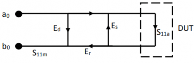
1-port calibration measures and removes 3 systematic error terms (directivity, source matching and reflection tracking) from reflection measurements. A directivity error (Ed) occurs when a portion of the generated signal—the incident signal—leaks to the reflected signal path. A source match error (Es) results from mismatch between the source port and the input of the DUT. The reflection tracking (Er) error is caused by the differences between the frequency responses of the reference receiver and the test receiver. The signal flow diagram for 1-port measurements is shown in Figure 1 where the a0 and b0 receivers are measuring the incident and reflected signals, respectively.

Figure 1: Signal flow diagram for 1-port measurement.
It can be seen in Figure 1 that the actual S11a of the DUT is different than the S11m that we measure with a VNA due to the presence of the 3 systematic error terms. Solving the signal flow diagram yields a bilinear relationship between the actual and the measured S11 as shown in Equation (1).
Calibration Standards for 1-Port Calibration

The bilinear relationship between the actual and the measured S11 of the DUT depends on 3 error terms as shown in Equation (1). Therefore, at least 3 independent calibration standard measurements are necessary to obtain the 3-error terms. The most commonly used calibration standards in 1-port measurement scenarios are SHORT, OPEN, and LOAD. These calibration standards provide very distinctive reflection coefficients that are helpful to solve the 3-term error model in the case of coaxial measurements.
However, a waveguide OPEN standard acts more as an antenna rather than a calibration standard. Therefore, for waveguide calibration, SSL (SHORT-SHORT-LOAD) standards are more often used as the calibration standards with the lengths of the two SHORT standards separated by at least ? 4 at the center frequency of operation. The differences in length of the two SHORT standards are necessary for effective variable separation of Equation (1).
Defining Waveguide Calibration Standards in CMT VNA
CMT VNAs support any standard waveguide calibration kit, and more recent software versions include a predefined assortment of widely used waveguide calibration kits. However, if a special waveguide calibration kit needs to be defined in the VNA, parameter calculations might need to be performed.
The required parameters for defining the calibration kit in the VNA include the waveguide cut-off frequency, the operating frequency range, and the delay of the offset SHORT calibration standards. These parameters can be calculated from the information provided in the waveguide calibration kit manufacturer’s datasheet.
The definition of calibration standard parameters for waveguide calibration kit is different than that of co-axial calibration kits. Waveguide does not support the TEM (Transverse Electro Magnetic) mode of wave propagation as do co-axial components; instead it supports TE (Transverse Electric) and TM (Transverse Magnetic) modes. TE and TM modes have limited bandwidth and in fact, none of these modes can propagate at frequencies below a minimum frequency known as the cut-off frequency. Therefore, the first parameter to be calculated is the cut-off frequency. The cut-off frequency depends on the largest dimension of the waveguide as shown in Equation (2).


Where a is the larger dimension of the waveguide. The lowest and the highest operating frequency are related to the cut-off frequency by Equations (3) and (4).
Once the cut-off frequency and the operating frequency range are determined, then the delay of the offset SHORT can be found from the datasheet provided by the manufacturer. Following is an example showing how to define a Flann WR229 waveguide calibration kit in the CMT VNA. This example is for the calibration kit highlighted in red, but the methodology is the same for all of them.

Figure 2: Datasheet of Flann waveguide calibration kits
Here the waveguide dimensions are: W = 58.17 mm and H = 29.083 mm.

The length of the offset SHORT calibration standards can be extracted from the datasheet.

All the calculated values can be inserted in the calibration standard table of the CMT VNAs. A screenshot of the calibration standard table is shown below.

Figure 3: A screenshot of the calibration standard table in CMT VNA.
Once the calibration standards are defined, the VNA is ready to be calibrated with waveguide calibration kit.
Example of 1-Port Measurement of a Waveguide Device with CMT VNAs
In this section, 1-port reflection (return loss) measurement of a waveguide band-pass filter will be demonstrated. The WR229 waveguide calibration kit has been used to calibrate out the three error terms as discussed in previous sections. The calculation of the calibration standard coefficients is as discussed in the last section. The DUT (Device Under Test) for this measurement was chosen to be an old M1052-4 from MITEC of unknown condition. The datasheet of the DUT is given below:

Figure 4: Datasheet of the MITEC M1052-4 band-pass filter
It can be seen in Figure 4 that S11 of the DUT should be -28 dB or lower in the frequency range of 3.7 – 4.2 GHz. The measured S11 of the DUT is shown in Figure 5. As can be seen, the device under test is not quite meeting its datasheet specifications.

Figure 5: Measured S11 of the waveguide band-pass filter
Conclusion
In this application note, calibration of CMT VNA with a waveguide calibration kit has been explained. The calculations for defining calibration standards in the VNA have also been presented. Finally, the VNA was calibrated with a WR229 waveguide calibration kit and the calibrated VNA was used to measure the S11 of a suspect band-pass filter.
Definition of a waveguide calibration kit involves a few calculations, so if you are not sure how to define a kit, please contact us and we will be glad to help! You can reach our support team at +1-317-222-5400 or support@coppermountaintech.com.
References
- P. Dunsmore, Handbook of Microwave Component Measurements, 1st ed., Wiley publications, 2012, ch – 3.
- http://www.flann.com/wp-content/uploads/2015/09/Waveguide-Calibration-Kits.pdf, retrieved on November 16th, 2015.
- http://www.gfsatcom.com/Datasheet/Mitec%20Rigid%20and%20Flexible%20Waveguide%20Component%20Data%20Sheet.pdf, retrieved on November 16th, 2015.