


Useful Radio Frequency Engineering Formulas and Charts
February 9, 2023Introduction
The following is a collection of essential formulas and charts for useful for Radio Frequency Engineering.
What is the Inductance of a Solenoid (Coiled Wire)?
The inductance of a solenoid is approximately:

Where r is the radius in inches, l is the length in inches, and n is the number of turns.
It may also be calculated more precisely from this equation (from Ampere’s Law) with similar results:

Where μ is free space permeability 4*10-7 H/m
n is the number of turns
A is the cross-sectional area in m2
l is the length of the coil in meters
What is the Inductance of a Straight Wire in Free Space?
Electronic circuits are often connected by wires. Small circuits may be connected by bond wires. A coaxial probe may have a short section of exposed center conductor, which is essentially a wire in free space. These all exhibit a certain amount of inductance. A chart of inductance of a straight wire in NanoHenrys per inch vs wire diameter or solid wire gauge is shown below in Table 1.

Table 1 – Inductance of a Straight Wire

Figure 1 – Free Space Wire Diam vs Inductance/Inch
Choosing a value of 20 nH/In as a rule of thumb is reasonable.
For example, if a simple probe is made by exposing 0.2” of a semi-rigid cable center conductor and adding a ground return on the side of equal length, then the total inductance of the exposed conductor plus ground is about 8 nH. The reactance of this inductance reaches 50 at 6.25 GHz which would be the effective 3 dB bandwidth of the probe.
What is the Capacitance between Two Parallel Plates?
The capacitance between two parallel plates is proportional to the area of the plates and the dielectric constant of the material between them, and inversely proportional to the distance between the two.

Where ε = εr * ε0
εr is the relative dielectric constant, 1.00059 for dry air at 1 atm and 20°C
ε0 is the permittivity of free space,
What is the Characteristic Impedance of a Coaxial Cable?
A coaxial cable is an RF transmission line which consists of a center conductor surrounded by a dielectric medium, a coaxial shield, and often an insulating plastic jacket.
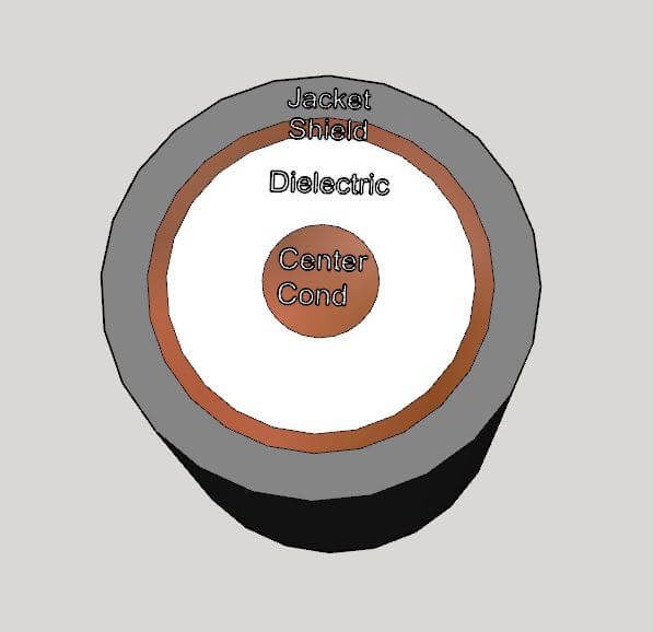
Figure 3 – Coaxial Cable
The inner conductor of the coaxial cable possesses an intrinsic inductance per unit length L’ just like the wire in free space. By virtue of the coaxial shield and the dielectric material, it also has a capacitance per unit length C’. The inductance and capacitance are distributed along the length of the cable, as shown in Figure 4 below.

Figure 4 – Inductance and Capacitance per Unit Length of a Coaxial Cable
If the inductance and capacitance per unit length are known, then the characteristic impedance of the cable is given by:
Low-loss dielectric materials such as PTFE are common. PTFE has a relative dielectric constant of 2.02 to 2.1, but this is commonly processed to create a PTFE foam with a significant amount of air, resulting in lower loss and a lower dielectric constant.
RF travels through the coaxial cable at the guide velocity vg, slower than the speed of light, c:
The relative velocity of propagation is expressed as the percentage of c or:

This number is approximately 65% for solid PTFE cables, and as high as 90% for low loss foamed PTFE. An air-line coaxial cable with only air as a dielectric would have a relative velocity of 100%.
The characteristic impedance of a coaxial transmission line may be calculated from:
Where Douter is the diameter of the outer shield to its inner surface, Dcenter is the diameter of the center conductor, and ∈r is the relative dielectric constant of the medium in between the two.
What is the Cutoff of a Waveguide?
A waveguide is a medium for the transport of RF signals. The medium can support many Transverse Electric (TE) or Transverse Magnetic (TM) modes. Normally, only the lowest order mode between the cutoff and the beginning of the next higher order mode is used, which is TE10 or TM11. Using a waveguide at a frequency where more than one mode is possible is not advised, as different modes have different group velocities.
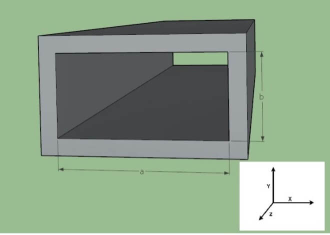
Figure 5 – Rectangular Waveguide
The low frequency cutoff of a rectangular waveguide for mode TEmn in terms of dimensions a and b is given by:
The formula is the same for TM modes, but TM10 is not realizable. The first transverse magnetic mode is TM11.
The component of the wave vector in the z-axis direction of propagation is given by:

And the phase velocity is:
And group velocity is:
For example, a WR-112 waveguide has dimensions, a = 2.85 cm and b = 1.26 cm. For TE10 mode, Fc is simply c/2a or 5.26 GHz.
The insertion loss of the WR-112 waveguide is shown below in Figure 6:

Figure 6 -WR-112 Waveguide Response Showing Cutoff
Typically, this waveguide is used from 7.05 to 10 GHz.
What are dBm?
RF signal power is often expressed in a logarithmic format. dBm refers to the ratio of the RF power to 1 milliwatt in logarithmic format. For instance, 1 Watt is 1000 milliwatts, so the ratio is 1000 and Log10(1000) gives 30 dBm. In general:
The RMS voltage of an RF signal in a characteristic impedance R is given by:
Some RMS and peak voltages in a 50Ω system are shown in Table 2.

Table 2- RMS and Pk RF Voltage vs dBm
Notably, the peak RF voltages at +10 dBm and +30 dBm are 1V and 10V respectively. This is useful to know when evaluating low frequency signal levels with an oscilloscope.
What is Thermal Noise?
First start with Boltzmann’s constant:
Boltzmann’s constant, k, gives the proportionality of the average kinetic energy of a particle in a system of particles at temperature K (degrees Kelvin). There will exist a statistical distribution of particles with higher or lower energy, but the average over a sufficiently great number of particles is useful for further calculations.
Charges within a resistor move about with thermal kinetic energy. If we consider a leaded resistor, then the axial component of current movement generates a voltage on the leads. This random axial charge movement creates an AC noise voltage on the resistor leads equal to:
Where k is Boltzmann’s constant
T is the Kelvin temperature
B is the bandwidth of the AC voltage measurement
R is the resistance of the resistor
The factor of 4 comes from the dimensional degrees of freedom accorded to the charges in the resistor and that only the axial component of movement contributes to output noise. The derivation is left up to the student.
For example, a 1 kΩ resistor will generate:
in a 100 MHz bandwidth at 22ºC
The thermal noise in a 50Ω environment at room temperature is -174 dBm in a 1 Hz bandwidth. An RF engineer should memorize this number. This comes from the noise power calculation:
What is Noise Figure?
Amplifiers suffer the effects of thermal noise and thermal charge movement within an amplifier appears on the output as added noise. This noise may be modeled as an external noise input to the amplifier. For example, the noise on the output of a perfect 10 dB amplifier in a 1 Hz bandwidth would be -164 dBm with no other signal input. If the actual noise output is -162 dBm, then the noise figure of the amplifier is said to be 2 dB. A chain of amplifiers will exhibit cumulative noise.

Figure 7 – Amplifier Chain with Noise
Cumulative noise figure is calculated as follows:
Where the gains and noise figures are evaluated in linear terms. That is:
A chain of three amplifiers, all with 10 dB of gain and 3 dB noise figure, would have a cumulative noise figure of 3.2 dB. It is clear from the formula that, as long as the gain of the first amplifier is relatively high, its noise figure will dominate the cumulative noise of the chain. A significant amount of attenuation introduced after the first amplifier would reduce its effective gain and allow the noise figure of the second amplifier to have a larger effect.
What are IIP3 and OIP3?
These two factors are used to characterize the linearity of a device, usually an amplifier. If two frequency signals (tones) are combined and amplified by a perfect amplifier, the output will simply be the same two tones with amplitudes increased by the gain. But amplifiers are not perfect, and always exhibit some degree of non-linearity.
An amplifier with a second order contribution will develop second harmonics of the two tones plus the sum and difference of the two tone frequencies. A third order contribution will develop intermodulation products on either side of the original two tones, equally spaced. If the input amplitude of both tones is increased by 1 dB, the output tones will increase by 1 dB and the two third order intermodulation products on either side will increase by 2 dB. If the two-tone input level is increased sufficiently, there is a theoretical output level where all four tones are the same amplitude. This level is called the third-order output intercept, or OIP3.
In practice, it is usually impossible to see all four tones at the same amplitude since gain compression usually sets in well before this can happen, but the theoretical level may be extrapolated from a measurement of the difference between the two main tones and the intermodulation products when they are at a much lower level, as shown in Figure 8.
Figure 8 – OIP3 Calculation
With knowledge of the OIP3 of an amplifier, you can calculate the level of the third-order intermodulation products for any given input level of two signals. This is important for determining the amount of interference created in adjacent channels in a communication system when two or more channels are active simultaneously.
The cumulative OIP3 of a chain of amplifiers like Figure 7 is given by:
Where the OIP3 and Gains are all converted to linear terms

Figure 9 – Amplifier Chain
Examining the formula shows that if the last stage has reasonable gain, then its OIP3 will dominate the cumulative system OIP3. The formula can also be expanded for any number of amplifiers.
The input IP3 or IIP3 is simply the OIP3 minus the gain of the amplifier. Mixers are generally specified with IIP3 while amplifiers are specified by OIP3.
What is a Reflection Coefficient?
Just as a beam of light might bounce off a sheet of glass, some or all of an RF signal may reflect from an impedance other than one equal to the characteristic impedance of the transmission line. If the characteristic impedance is Z0 and the encountered impedance is Z, then:
If the encountered impedance is complex, then the reflection coefficient is also complex. If Z = Z0, then Γ = 0 and there is no reflection. If Z is 0, a short, then Γ = -1 and the reflection is total but inverted. If Z is infinite, an open, then Γ = 1 and again the reflection is total but in phase.
For complex impedances, the reflection coefficient will also be complex, and may be expressed as a vector with magnitude less than one and some angle such as 0.5∠53°. It can be expressed in Real/Imaginary Cartesian coordinates as well, such as 0.3+j0.4 which is the same vector. Figure 10 depicts a reflection coefficient as a vector on a polar chart.
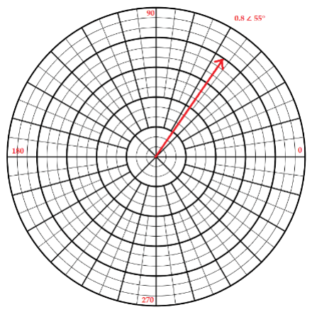
Figure 10 – Vector on a Polar Chart
What is Return Loss?
Return loss is the name for the reflection from a Device Under Test, or DUT. As a specific example, an RF signal is launched into a transmission line connected to the DUT. If the input impedance of the DUT is not equal to the characteristic impedance of the transmission line, there will be a reflection. Reflected energy is not available to pass into the DUT and is returned to the source and lost. The impedance mismatch determines the reflection coefficient (see above), and the return loss may be calculated for it.
Return loss is normally expressed in dB and as a positive number. If a VNA measurement of the DUT is performed with Port 1 connected to the DUT input, then S11, as displayed in Log-Mag mode, would be the return loss. S11 for a passive device will always be negative but, by convention, return loss is expressed as a positive number. If S11= -20 dB, then the return loss would be expressed as 20 dB.
What is VSWR?
VSWR, or Voltage Standing Wave Ratio, is found from the reflection coefficient:
If a transmission line is feeding a DUT and there is an impedance mismatch between the DUT input impedance and the characteristic impedance of the line, there will be a nonzero reflection coefficient Γ.
The existence of a reflection on the transmission line gives rise to constructive and destructive interference along its length and stationary peaks and valleys in the RF voltage will occur. The ratio between the maximum and minimum RF voltage along the length is equal to the VSWR. If there is no variation, then the VSWR = 1 (or often written 1:1), and there is a perfect match with no reflection.
The magnitude of the reflection coefficient may be found from:
What is the Inverse of Impedance, Reactance, and Resistance?
The inverse of impedance is admittance. Traditionally, impedance is expressed as R+jX, where R is resistance and X is reactance, both in units of ohms. Admittance is the inverse of impedance and is expressed as G+jB, where G is conductance and B is susceptance. Conductance is the inverse of resistance, and B is the inverse of reactance. Both have units of mhos.
Capacitive and inductive susceptance are given by:
What is a Thevenin-Norton Transform?
At a given frequency, a series impedance may be transformed into an equivalent parallel impedance and vice versa. This transformation is useful for impedance-matching calculations. Given a series impedance R+jX or a parallel admittance G+jB:

Figure 11 – Thevenin and Norton Transforms
How Can I Use an Inductor and a Capacitor for Impedance Matching?
For the simplest case of real input, Rin, to real output impedance Rout, there are two possibilities: Rin > Rout or Rin < Rout. The two L topologies to accomplish this are:

Figure 12 – Matching Topologies
If we assume the Zout is real R2, Zin is real R1, and R2 > R1 (the left-side topology in Figure 9) we can use the Norton transformation to get:
For example, to match R1 = 50Ω to R2 =1000Ω at 100 MHz:
choosing the positive root to use a shunt capacitor for a lowpass implementation, then:
For R2 < R1, simply swap R2 for R1 in the above calculations. The useful bandwidth of the match will depend on the ratio of R2 to R1. Extreme transformations result in very narrow bandwidth results. A broader band match may be implemented using more L-C elements [1] [2].
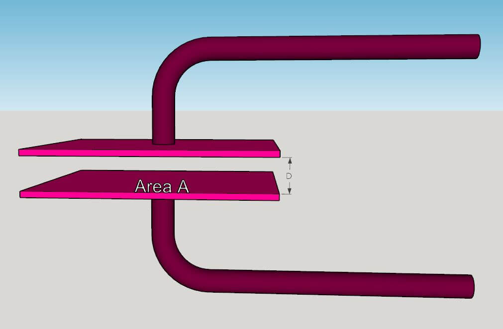
What is Sheet Resistance?
The resistance of a length of metal is given by:
Where ρ is the bulk resistivity of the material, L is the length, and A is the cross-sectional area as shown in Figure 13. Sheet resistance Rs is given by:
If a material has a sheet resistance of 10 ohms/square and is cut into a square shape (L=W), then the measured resistance from one edge to opposite edge will be 10Ω regardless of the size of the square.
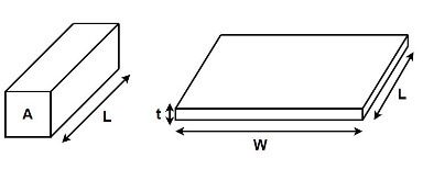
Figure 13 – Sheet Resistivity
What is the Formula for the Discrete Fourier Transform?
For a sequence of complex numbers in the time domain xn, the discrete Fourier Transform Xk is given by:![]()
For frequency analysis of a time domain data set, window the data to reduce sin(x)/x artifacts in the result.
What are Transfer Parameters?
S-parameters matrices are a convenient way to characterize devices, but it isn’t possible to multiply them for cascaded devices. Fortunately, S-parameters can be transformed into transfer parameters, which can then be multiplied in the usual way. The conversion is:
![]()
And the inverse formula is:![]()
References
[1] G.L. Matthaei, “Tables of Chebyshev impedance–transforming networks of low-pass filter form”, Proceedings of the IEEE, Vol 52, Issue 8
[2] R.M. Fano, “Theoretical limitations on the broadband matching of arbitrary impedances”, Journal of the Franklin Institute, Vol 249, Jan 1950, pp 57-83