

What are the Basics of a VNA?
August 29, 2023How does a VNA Work ?
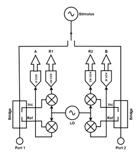
A block diagram is an excellent starting point to understanding vector network analyzer basics. The image below depicts a simplified block diagram for a USB vector network analyzer. The Port 1 and Port 2 bridges shown are the components which separate the forward and reverse traveling RF waves. Receivers R1 and R2 pass only a sample of the wave exiting Ports 1 or 2. Receivers A and B pass only a sample of waves entering Ports 1 or 2. A vector network analyzer uses only three active receivers at any time. Receiver R1 is active when the stimulus is switched to Port 1, and R2 is active when it is switched to Port 2.

Figure 1: Typical VNA Block Diagram Image
When the stimulus signal is switched to Port 1, the magnitudes and phases of the signals on reflection receivers A and B are normalized to stimulus receiver R1. In this way, the absolute output power of the stimulus is irrelevant. Similarly, when the stimulus is switched to Port 2, measurements A and B are normalized to receiver R2. The performance of a linear DUT can be predicted under any source and load impedance with knowledge of transmitted and reflected signals (S-parameters) from both sides.
What are the applications of Vector Network Analyzers?
CMT VNAs are being utilized by engineers in many different industries including defense, automotive, materials measurement, medical, broadcasting, and telecommunications. There are many applications for VNAs across these industries. One example is the characterization of RF amplifiers for gain, return loss, P1dB, output match, and stability. All of which are vital to the design and performance of an amplifier.
![]()
VNAs are also used to evaluate the properties of an RF filter. VNAs can be used for s21 parameter insertion loss, or S11 return loss measurements. Antennas are also often evaluated with a VNA. Reflection measurements are most suitable for evaluating antenna performance.
VNAs are commonly used in the production of RF cables and waveguides as well. 1-Port VNAs are a convenient tool for verifying proper cable performance. Time Domain mode is specifically used to verify characteristic impedance over distance which enables cable manufacturers to check for damage or moisture ingress. Waveguide transmission lines can also be measured with a suitable coaxial to waveguide adapter by using Time Domain.
VNAs are also adept at measuring the dielectric properties of materials. Millimeter wave VNAs are the best option for this type of measurement. A sheet of a material to be measured is held in a frame between two antennas connected to a VNA as in the image below. Two lenses focus the beam to transform the circular wavefronts into plane waves. The dielectric properties of a sheet material may be measured in this way.
What is the difference between SNA and VNA?
A spectrum analyzer is intended to visualize the spectral components of input signals. Its architecture is optimized for clean visualization of signals without visible side-lobes or spurious signals. A vector network analyzer is intended to only measure its own stimulus signal, and its architecture is optimized for fast measurement speed. A VNA can be used as a rudimentary spectrum analyzer, but it isn’t optimized for the task. To do so would require a much more complicated architecture and would significantly increase the product cost.
Why are VNAs so Expensive?
It is the combination of broadband high frequency components like these, plus the FPGA, which overwhelmingly contribute to the cost of goods for the VNA.
However, if the VNA is developed with integrated microwave VCO/PLL sources rather than a multiloop phase locked system with separate VCOs and a Direct Digital Synthesizer (DDS) to achieve the small frequency steps, it can be implemented at a lower cost. The economical Compact models from CMT are designed in this way. The Cobalt models use the more sophisticated signal synthesis methods and achieve higher dynamic range as a result.