


Amplifier Measurements
August 31, 2022Introduction
RF amplifiers are an important part of many RF systems designs and it is often required to make Vector Network Analyzer (VNA) measurements of them to verify function and ensure suitability for the intended application. Measurement of these devices present challenges – among them, the need for a pre-amplifier to produce sufficient drive level for a Power Amplifier (PA), handling of the output power in a way that properly loads the PA without damaging the input port of the VNA, and determining calibration methods to achieve acceptable accuracy. Additionally, one may want to measure the output impedance of the amplifier while it is being driven with an input signal which excites it to its nominal output level. Output power vs. input power may be measured to determine amplitude linearity. Harmonic distortion, AM to AM, and AM to PM conversion may be analyzed. All these measurements are possible with a VNA, but a proper setup is needed to achieve accurate results.
Low-Level Amplifier Measurement
A signal amplifier might have gain from 5 to 25 dB or more. 1 dB compression of the output may occur anywhere from -10 to +20 dBm. These are typical ranges, but amplifiers with 1 dB compression above +20 dBm begins to approach PA territory. How are these measurements made?
Gain and Return Loss
To measure the gain of an amplifier, it is important to understand how to set up the VNA to make a precise measurement. Assuming that the measurement is made from port 1 to port 2 for a measurement of S21 as in Figure 1, it is necessary to ensure the input level to port 2 is optimal.

Figure 1 – Low-Level Amplifier Measurement
The receivers of the VNA perform best with input levels between -10 and 0 dBm. Below -10 dBm, trace noise begins to steadily increase, but if the input level is arbitrary, it is best to place it in this range. Above 0 dBm – for most VNA models – the receivers will approach compression and accuracy will suffer. For the example in Figure 1, the stimulus output level from Port 1 has been reduced from the 0 dBm default level to -30 dBm. Note that the VNA calibration should be performed with the stimulus power set to 0 dBm. Stimulus power may then be reduced after calibration without loss of accuracy. It is a simple matter to measure amplifier return loss, gain, reverse isolation, and output match (S11, S21, S12, S22).

Figure 2 – Amplifier

Figure 3 – Amplifier Measurement
Figure 3 shows the four S-Parameter measurements of the amplifier shown in Figure 2.
1 dB Compression
The 1 dB compression point is easily found by performing a power sweep at a chosen frequency. In Figure 4, the input power is swept from -30 to -10 dBm. The top trace shows the S21 reading, which falls off when the output begins to compress. Where S21 falls by 1 dB on the top trace, the bottom trace shows the input and output power of the amplifier. The 1 dB compression point is 8.7 dBm at 1 GHz. The bottom trace is the raw “B” receiver measurement which gives the absolute, un-ratioed input power to Port 2. This measurement was made after performing power and receiver calibration using an external power meter. Receiver calibration improves the raw receiver accuracy to about ± 0.1 dBm. Without it, the power accuracy would be ±1.5 dB. Normal S-Parameter measurements do not require port power or receiver calibration, as they are ratioed values and small variations in stimulus power are unimportant.

Figure 4 – Power Sweep
For the power calibration, the R&S NRP-Z was first chosen from System/Misc Setup/Power Meter. Then, Power Calibration was chosen from Calibration/Power Calibration. Note that the chosen power meter series is shown at the top of the menu bar. The power meter was then attached to the end of the test cable attached to Port 1 of the VNA. First, the Power Sensor Zero Correction was chosen. The VNA turned off the RF power and the power meter was zeroed. Then, with Port 1 selected, the “Take Cal Sweep” was initiated. The VNA sweeps through all chosen frequencies and performs the calibration. This should be done with the VNA stimulus power set to 0 dBm. Lower power levels may be chosen, but the calibration time will increase dramatically and be less accurate.
After the Port 1 power calibration is complete, the receiver on Port 2 may be calibrated. If the 1dB compression point of the amplifier exceeds +5 dBm then an attenuator pad should be added to the port to limit the input power to this level or less. Proceed to Calibration/Receiver Calibration. Select Port 2 and Source Port 1 and connect the two test cables together with a thru. Now, press the “Calibrate Test Receiver” button and the power accuracy of the input receiver on Port 2 will be corrected (even if a pad has been added). It is important to perform the power calibration on Port 1 prior to the Port 2 receiver calibration, so that input to Port 2 is a known corrected value. The P1dB measurement requires this calibration since the measurement uses unratioed raw receiver values.
A plug-in for 1 dB compression point measurement is also available here.
Power Calibration at High Power Levels
If you navigate to Stimulus/Power/Port Couple [Off]. Then select Port Power. You will be able to set the output power of Port 1 or Port 2 to levels available from the VNA. If a Pre-Amplifier is placed on Port 1 to boost the stimulus level, this can be entered in the power offset. If the amplifier has 30 dB of gain, enter that in the offset field. Enter the desired combined output in the Port Power field, and the VNA source power will change accordingly. The VNA power display at the bottom of the screen will indicate the correct power level of each port.

Figure 5 – Power Offset Entry
If a power meter is capable of handling the new output power, then a power calibration can be performed with the pre-amp in place. In the case where the amplified output power is too high for the power meter, a pad can be installed between the pre-amp and the power meter. To compensate for the pad, navigate to Calibration/Power Calibration/Loss Compen, enter the pad value at desired frequencies in a table, and turn Compensation [ON]. Compensation between entered points will be interpolated by the VNA. If measured values for the pad are available, a simple program script can generate the table. Use the format below and save the file with an “lct” file extension.

Figure 6 – Loss Compensation for 30 dB Pad
With the pad in place, perform the VNA power calibration normally. Remove the pad when calibration is complete. After this process, the VNA will display the higher stimulus power on the screen and it will be calibrated.
Loss Compensation file format:
[Loss Compensation]
Count=4
Frequency[0]=10000000
Loss[0]=30
Frequency[1]=20000000
Loss[1]=30.5
Frequency[2]=30000000
Loss[2]=30.6
Frequency[3]=40000000
Loss[3]=30.7
Frequencies are in Hz, and the Loss values are the attenuation of the pad.
Harmonic Distortion
The harmonic response of an amplifier may be measured easily using the frequency offset function available in all Copper Mountain Technologies VNAs except for the “M” series. It is important to understand that the VNA itself emits harmonics of the stimulus. Typical harmonic levels are -20 dBc for compact models like the S5065 and -25 dBc for the Cobalt series like the C1209. For normal VNA measurement, the receiver tracks the stimulus signal and only sees what is within the IF bandwidth at that frequency. Spurious signals and harmonics are normally of no consequence. The harmonic output of the VNA and potential harmonic distortion of the receiver will interfere with making an accurate harmonic measurement though. To mitigate this, add a bandpass or lowpass filter to the stimulus output and a 10 to 20 dB pad to the receiver input.
As an example, a bandpass filter with passband from 433.5 MHz to 592 MHz will be used to filter the stimulus driving the 2 GHz amplifier from above and the third harmonic from 1300.5 MHz to 1776 MHz will be evaluated. The filter in Figure 5 has a dB or two of loss between 433.5 and 592 MHz. The rejection of the third harmonic from 1300.5 to 1776 MHz is at least 120 dB, so stimulus harmonics will not affect the measurement.

Figure 7 – 500 MHz Filter Response
With the DUT amplifier in place and -30 dBm stimulus, the input to Port 2 will be + 2 dBm. Port 1 power calibration is performed from 433.5 MHz to 1776 MHz, at 0 dBm covering both fundamental and 3rd Harmonic frequencies. Receiver calibration is then performed on the Test Receiver of Port 2 over this range, with Port 1 and Port 2 connected by a thru. Next, the 500 MHz filter is put in place of the thru and the frequency range is changed to 433.5 to 592 MHz and power calibration is performed once again on the output of the filter. Now the Port 2 receiver is calibrated over the broad range, and Port 1 power is corrected to 0 dBm on the output of the filter. The VNA frequency range is now changed to 1300.5 MHz to 1776 MHz, the third harmonic frequencies, and the Frequency Offset mode is engaged with Port 1 set to 433.5 to 592 MHz and Port 2 set to 1300.5 to 1776 MHz. With the stimulus power out of the filter increased slightly to + 2 dBm, the Port 2 receiver harmonic distortion is in the range of -75 dBm as shown in Figure 6. This is high enough to add some error to amplifier third harmonic measurements in the -45 dBm range, so a 10 dB attenuator is added to Port 2 and the new measurement with -8 dBm into the port shows -105 dBm third harmonic response for the receiver as shown in Figure 7. This is acceptable.

Figure 8 – Receiver 3rd Harm Distortion at +2 dBm

Figure 9 – Receiver 3rd Harm Distortion at -8 dBm
Now that the measurement system has been fully verified, the third harmonic distortion of the amplifier may be measured. First, with -30 dBm input drive, the fundamental output power of the amplifier is measured and stored in memory. Then, receiver offset mode is engaged and subtracted from the fundamental output level using data/memory to obtain the third harmonic distortion relative to the fundamental power in dBc as shown in Figure 8. The calibration steps are shown in Figure 9. As described earlier, the power is calibrated twice – once to allow calibration of the Port 2 receivers through the pad to 1776 MHz and a second time to calibrate the power within the passband of the bandpass filter with the filter in place to correct for the insertion loss. Turn off the previous power calibration before performing the new one.

Figure 10 – Amplifier 3rd Harmonic Distortion, dBc

Figure 11 – Harmonic Measurement Setup
Rollet’s Stability factor, K
The K factor of an amplifier is an indication of stability. A K factor greater than 1 at a frequency means that the amplifier is unconditionally stable. Where the gain of an amplifier is greater than , and the K factor is less than 1, there exists a complex load which creates an input reflection coefficient with a negative real part or a complex source impedance on the input which creates a complex output impedance with a negative real part. Oscillation will occur when the gain is greater than 1 and an amplifier input or output has an impedance with negative real part.
For a full two-port S-Parameter measurement, the K factor is:

Equation 1 – K Factor
Where the determinant:
We know from Mason’s rule (Reference 1) that the complex input reflection coefficient Γin of an amplifier loaded by ΓL is given by:

Equation 2
The right-hand side represents a bi-linear circular or ovoid shape centered at S11. For very high isolation amplifiers, with small S12, this simply reduces to S11. For non-trivial S12, the input reflection coefficient of the amplifier moves about S11 as the complex load ΓL changes and the real part of Γin would be negative for K<1.
A “plug-in” which calculates the K factor may be downloaded from the Copper Mountain Technologies website. Other plug-ins are available as well. Simply download the plug-in and save it to the C:\VNA\S2VNA\Plugins (Or S4VNA) folder or wherever the VNA software is installed. After re-starting the S2 or S4VNA software, navigate to System/Plugins to find the application and run it.
Using this plug-in, the K factor of the amplifier in Figure 2 with S-Parameters shown is Figure 3 is plotted below in Figure 10.

Figure 12 – Amplifier K Factor
The K factor approaches 1 at 1 GHz but the amplifier appears to be unconditionally stable.
To illustrate graphically, the output match of an amplifier causes the input impedance change according to Equation 2. The effect of the output match can be mapped between a pair of Smith charts, where the output match is located on the smaller chart and the corresponding input match is found on the larger chart as shown in Figure 11. If the smaller chart is wholly contained within the larger, then it is impossible to find an output match which maps to a negative real impedance on the input. On the other hand, if part of the smaller chart passes outside the larger, then there exists a range of complex output impedances which will cause the input impedance to have a negative real part and oscillation will occur. The first case would be unconditionally stable and have a K of greater than 1 and in the second case, conditionally stabile with K less than 1.

Figure 13 – Mapping Output Load to Input Match, Stable and Potentially Unstable Amplifiers
A conditionally stable amplifier may still be used in a circuit as long as its load is managed.
Third Order Intermodulation Output Intercept, OIP3
The OIP3 of an amplifier is measured with a pair of CW signals, also called “tones”. A perfectly linear amplifier with two tones on the input would faithfully reproduce them on the output without distortion. No amplifier is perfectly linear however, so a number of extra frequency products are created. In particular, second order effects result in the sum and difference frequencies of the two tones and third order effects result in a pair of intermodulation (IM) tones on either side of the initial pair, equally spaced. For evaluation of a multichannel radio system, the tones are spaced at the channel separation so the level of interfering IM’s falling into adjacent channels may be evaluated. Amplifiers for digital systems might also be evaluated this way but, generally speaking, Error Vector Magnitude (EVM) is used instead and a VNA is not used for EVM measurement.
Due to the way the trigonometric math works out, the two IM tones increase or decrease in amplitude at three times the rate of change of the two equal fundamental tones. At some fundamental tone amplitude, the two IM tones would be equal in amplitude as in Figure 12. In practice, this doesn’t actually occur, since the amplifier would go into hard limiting well before that, but the level may be extrapolated from the level of the fundamental tones compared to IM tones while they are 40 to 60 dBc lower. This extrapolated output level where all four tones would be of equal amplitude is called the 3rd Order Output Intercept and is a figure of merit for amplifier linearity.
It is important to ensure that the measurement is evaluating the OIP3 of the DUT and not the Input IP3 (IIP3) of the VNA. Add a pad to the VNA receiver input to keep the input level below -10 to -15 dBm to ensure that this is the case. Additionally, poor isolation of the combiner used to put the two tones together may allow one tone to cross over and enter the output of the other tone source and mix to create spurious intermodulation tones. Add pads to the outputs of the two tone sources if necessary to prevent this. If possible, test the setup by performing a measurement without the DUT in place and with the signal levels turned up to the level which would occur at its output. Any IMs seen in this case are either generated by the VNA receiver or source to source crossover through the combiner. These spurious IMs need to be at least 20 to 30 dB below what the DUT will generate for best accuracy. Add pads as needed.

Figure 14 – OIP3
A second stimulus source is required to generate two tones for the OIP3 measurement. 4-Port VNAs from CMT, such as the C1409 and C1420, have auxiliary sources which may be used for this purpose. Here is a video demonstration and an OIP3 plug-in is available for automating this measurement and is available here.
The two tone measurement is made using the VNA in frequency-offset mode. The two stimulus tones are held constant while the receiver is swept over a range which includes the two tones and IM products. The frequency offset mode is a standard feature of all CMT VNAs except the “M” series. For a 2-Port VNA such as the S5065, one tone could be generated by Port 1 in zero span (CW frequency, not swept) and a second tone by an external generator with the Port 2 receiver sweeping over the range. A 4-Port VNA such as the C1409, can generate both tones and make this measurement without the need for an additional source as in Figure 13.
For advanced modeling of an LDMOS or HEMT amplifier, try the IVCAD software from AMCAD Engineering. In combination with a Copper Mountain Technologies VNA, one can accurately model active non-linear devices. Load-Pull measurements can also be made with IVCAD and hardware from Maury Microwave. Focus Microwaves also supports non-linear modeling of devices with CMT VNAs.

Figure 15 – 4-Port VNA for OIP3 Measurement (“X” is 1, 2 or 4)
AM to PM Conversion
If the output phase of an amplifier is measured at a particular frequency while sweeping the input power, it is possible to measure AM to PM conversion. The greatest phase changes occur as the output level approaches compression. To do this, power calibration was performed on Port 1, and then Receiver calibration was performed on the Reference receiver of Port 1 and the Test receiver of Port 2 with a thru installed between Ports 1 and 2. The absolute measurement R1(1) accurately gives the input power and absolute measurement B(1) gives the output power. Figure 14 shows a typical measurement. The input and output power, S21 magnitude and phase are all shown. As the output power of the amplifier approaches + 10 dBm there is a significant drop in the phase. If the amplifier were driven with an AM modulated signal with the carrier at + 10 dBm, there would be a significant amount of phase modulation added to the signal.

Figure 16 – AM to PM measurement
The VNA Receivers
Figure 17 depicts a block diagram of a 2-Port VNA. Each port has two receivers associated with it, one to sample the level of the incident signal leaving the port and the other to measure signals entering it. There is a long legacy of names associated with the receivers and it can be confusing. The receiver which measures the incident signal is called the “Reference” receiver and designated by the letter “R”. It is called the reference receiver because the phases and amplitudes of signals received by this port as a reflection or other ports as transmissions will be referenced to it. The reference receivers are denoted by R1 and R2 or R1 through R4 in the Absolute measurement section of the S2VNA or S4VNA UI software and by “Ref 1”, “Ref 2”, “Ref 3” and so forth on the front panel access ports of a Direct Receiver Access (DRA) VNA.
The receivers which measure signals entering a port are either denoted by “A” and “B” for Ports 1 and 2 of a 2-Port VNA or T1 through T4 for a 4-Port VNA in the absolute measurement menu of the UI. The “T” stands for “Test” in this case. These receivers may also be called “Measurement” receivers and denoted by “Meas 1”, “Meas 2”, “Meas 3” and so forth on the front panel of a DRA VNA. These receivers have three naming conventions, “A” and “B” for 2-Port VNAs, “T” for 4-Port and higher VNAs, and “Meas” for the front panel connections of a DRA VNA. The UI selections for receiver measurements are shown in Figure 15 below. DRA front panel designations are shown in Figure 16.

Figure 17 – Receiver Measurement Nomenclature

Figure 18 – 2-Port and 4-Port DRA Connector Layout
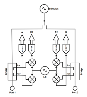
Figure 19 – 2-Port VNA Block Diagram
Using an External Coupler
The “bridges” within the VNA shown in Figure 17 separate incident and reflected signals, although it is sometimes desirable to make a measurement with the bridge placed inside the signal chain, such as when a pre-amplifier is used to drive a DUT at a higher level than the VNA produces. With the pre-amplifier in place, it is not possible to measure the return loss or S11 of the DUT using the bridge within the VNA. To make this measurement, an external coupler may be put in place between the pre-amplifier and the DUT as in Figure 18. To calibrate this configuration, choose “Response Thru” calibration from the menu. Making sure to select the appropriate calibration kit, detach the connection from the DUT, attach the calibration Open and push the “Thru” button. Then, attach a load to the end of the cable and push the “Isolation” button.
This calibration corrects the directivity error of the coupler and compensates for the coupling loss. The source match presented to the DUT from the output of the pre-amp is not corrected, so it is important to choose a pre-amplifier with a good output match. After calibration is complete, the S21 measurement on the VNA will correspond to an S11 measurement of the DUT and S11 will be a measurement of the pre-amp input which is likely not of interest.
Use this configuration if it is necessary to measure the return loss of a “Hot” cable (one with high level RF signals that would otherwise damage the ports of the VNA). In this case, the pre-amp isolates Port 1 and the coupling loss of the coupler isolates Port 2 from being overpowered. A pad may be added between the pre-amp and the coupler to protect it from large signals as well, as shown in Figure 19.
A VNA with Direct Receiver Access is required to perform a more sophisticated measurement with full 2-Port calibration.

Figure 20 – External Coupler Measurement

Figure 21 – “Hot” Antenna Measurement
Direct Receiver Access
The 9 and 20 GHz Cobalt VNAs from Copper Mountain Technologies may be ordered with the Direct Receiver Access (DRA) option. On each port, the Incident and Reflected ports of the bridge along with the Stimulus Source are broken out to “Loops” on the front panel, as shown in Figure 20. The Reflection receivers are denoted by “Meas 1”, “Meas 2” and so forth on the front panel and the incident signal receivers are denoted by Ref 1”, “Ref 2” and so on.
With the receivers broken out in this way and after removing the loops, it is possible to feed them with the forward and reverse coupled ports of a directional coupler. Full 2-Port calibration is performed in the usual way but on the output of the coupler or the cable attached to its output. Of course, calibration will only be accurate within the operational frequency range of the chosen coupler. With signals going directly into the receivers, note the maximum DC and signal levels allowed for the DRA ports. The maximum operating signal levels are shown in Table 1. Take special note of the DC voltage limitation. Applying any DC voltage to the Ref or Meas receivers will damage the hardware.

Table 1

Figure 22 – Direct Receiver Access (DRA) Loops
A 2-Port VNA with Direct Receiver Access can be connected as in Figure 21 to measure a DUT on the other side of a pre-amplifier. The “Ref 1” input samples the incident signal and “Meas 1” samples the reflected signal from the DUT. To perform a full 2-Port calibration in this configuration, Open, Short, and Load standards are connected to the two calibration plane points and then a thru is connected between them. Again, it is important to verify that the nominal input levels conform to the recommendations of Table 1 to ensure accurate measurement and prevent damage to the receivers.
If the DUT is also an amplifier with high output level, an attenuator may be needed on the Port 2 input to prevent damage. For best accuracy, the input level to Port 2 should be near 0 dBm. For full 2-port calibration, a 10-12 dB attenuator can be accommodated. Above this, the calibration will be noisy and measurement uncertainty will increase rapidly. It is not possible to perform the One-Port, Open, Short and Load calibration through a 20 dB attenuator. If an attenuator of this magnitude is required, use One Path, 2-Port calibration. This will not correct for Port 2 load match, but if the attenuator has good return loss, this is of no consequence. (Poor load match results in small ripples in transmission measurements). This calibration method will also only allow measurements of S11 and S21.

Figure 23 – 2 Port DRA for Pre-Amp
DUT Output Measurement with DRA
The measurement of Figure 21 cannot make S22 measurements accurately if the attenuator required to protect the port input from RF power is 20 dB or more. Adding an additional coupler on the output can alleviate this problem. In Figure 22 below, the output of the DUT that may be emitting several watts of power is not connected directly to Port 2. Instead, the power is safely delivered to a load. The coupling port of the output coupler reduces the level to the input of the Measurement receiver to a safe level and pads might be added to the coupling port to reduce this level even further. Once again, this configuration must be calibrated with the 2-Port, One-Path method. S11 and S21, may be measured, but not S12 or S22. It is particularly useful when a power RF load is available but there is no appropriate power attenuator.

Figure 24 – Output Coupler for High Power Output
Full 2-Port measurements may be made using a pair of couplers and judiciously chosen pads to keep signal levels within a reasonable range. Figure 23 below shows the forward and the reverse measurement signal levels. The 30 dB pad on the right-hand side is necessary to prevent damage to the Port 2 input. The 20 dB amplifier ahead of it boosts the stimulus signal to compensate for the loss and provides additional isolation. The 15 dB pads on the output coupler are needed for the forward measurement but result in a much smaller signal to the receivers in the reverse measurement. Theoretically, if the forward measurement was not needed at the same time as the reverse measurement, one could remove the 30 dB pad, the 20 dB amplifier and the two 15 dB pads on the coupler. A 1-Port calibration would be performed at the calibration plane on the left side of the output coupler and the output match of the power amplifier could be measured while it is not being driven. (Note that a 1-Port calibration is required here since a 2-Port calibration will always switch the stimulus source back and forth between Ports 1 and 2 even when only S22 is being displayed). Doing this would be quite dangerous, as the power amplifier will almost surely emit a damaging signal at some point, perhaps when power is first applied. It is better to be cautious.
Very often, the output match of an RF Power amplifier changes between its driven and quiescent states. If it is necessary to measure S22 with amplifier excitation, an off-frequency signal must be applied to the pre-amp on the left-hand side. This signal must be far enough away from the S22 measurement frequency to assure that its phase-noise tail does not interfere, likely many megahertz below the start frequency of the sweep or above the stop frequency. A separate generator might be used for this, or the auxiliary source available on Cobalt 4-Port VNAs could be utilized as shown in Figure 24. The offset signal could be applied to the “Source 1” DRA connector after removing the loop. This is called a “Hot S22” measurement and requires the careful balancing of pad values shown since RF power is present in both directions simultaneously.

Figure 25 – Full 2-Port Measurement

Figure 26 – Using Auxiliary Source for Hot S22 measurement
Pulsed RF Amplifier Measurement
An RF power amplifier may be measured using pulse modulation. The S5180B 18 GHz VNA from CMT contains a pulse modulator (Figure 25) which allows the stimulus signal to be modulated with pulse widths as narrow as 500 nS. If a 10 Watt power amplifier is excited with 10 μS pulses at a 1 mS repetition rate, the average power is only 1 milliwatt. This amount of power is easily handled by the front end of the VNA. Additionally, the 1 mW power dissipation of the PA would allow its measurement without the need for a heat sink or fan.
At the highest IF bandwidth, the S5180B can make an S-Parameter measurement in about 4 µS. This can be done completely within the pulse in the synchronous triggering mode as long as the pulse width is greater than 5 µS or so (Figure 26). Measurements of narrower pulses can be accommodated in the asynchronous mode where the measurement period is set long enough to include at least ten full pulses (Figure 27).

Figure 27 – S5180B Pulse Modulation

Figure 28 – Synchronous Pulse Measurement

Figure 29 – Asynchronous Pulse Measurement
All other CMT VNAs except the TR1300/1 are capable of making pulsed measurements either asynchronously or synchronously with an external trigger. The modulation of the VNA stimulus must be done externally, which is simple to do with a GaAs switch as shown in Figure 28. The VNA can be set to make a measurement on either the rising or falling edge of the trigger pulse. The trigger edge to measurement start delay can also be adjusted to avoid distortion at the beginning of the pulse as in Figure 26.

Figure 30 – Ext Pulse Modulation
For synchronous pulse measurement, choose “Event [On Point)” from “Stimulus/Trigger/Ext Trigger” and set the trigger polarity appropriately. Ensure that the measurement can be completed within the pulse width time. This measurement time is approximately equal to 1.3/IF bandwidth. Set the IF bandwidth to a higher value to reduce the measurement time if necessary. If the pulse width is too narrow and the measurement cannot complete within it, set the IF bandwidth lower such that ten pulses occur within the measurement period and use internal triggering of the VNA to make an asynchronous measurement. S21 measurements will be lower by 20*Log10(Pulse Duty Cycle), so it will be necessary to add this correction in post processing of the data. The S5180B with its internal pulse modulation makes this correction automatically.
Conclusion
A VNA is an essential tool for the measurement and characterization of amplifiers, both low-level and high power. With the appropriate set-up, one can measure gain, return loss and output match, P1dB compression, AM to PM conversion, harmonic distortion, stability and OIP3. These are important criteria to understand for the design of sophisticated circuits. Copper Mountain Technologies provides the equipment and technical solutions for making these measurements. Visit us at www.coppermountaintech.com to see our full line of Vector Network analyzers from 1.3 to 330 GHz, peruse our many educational videos and white papers like this one or contact our Sales organization for a quote or demonstration.
References
- Mason, Samuel, “Feedback Theory – Further Properties of Signal Flow Graphs”, Proceedings of the IRE (Volume: 44, Issue: 7, July 1956)