What are dBm?
March 22, 2023RF signal power is often expressed in a logarithmic format. dBm refers to the ratio of the RF power to 1 milliwatt in logarithmic format. For instance, 1 Watt is 1000 milliwatts, so the ratio is 1000 and Log10(1000) gives 30 dBm. In general:![]()
The RMS voltage of an RF signal in a characteristic impedance R is given by:![]()
Some RMS and peak voltages in a 50Ω system are shown in the table below.

Table – RMS and Pk RF Voltage vs dBm
Notably, the peak RF voltages at +10 dBm and +30 dBm are 1V and 10V respectively. This is useful to know when evaluating low frequency signal levels with an oscilloscope.
See this and more important radio frequency charts and formulas in this comprehensive application note.
Related Post

Can I Use a VNA as a Signal Generator?
September 12, 2023
Yes! We often are asked about using a vector network analyzer for another purpose, as test equipment budgets may need to stretch. But the answer to this question is yes, you can use a VNA as an additional signal source for testing. Below are some basics of how to do it but there is a more robust application note available here to review for more details.You can set the sweep range to “Zero Span” and set the frequency to the desired value and the VNA will output a constant frequency tone. However, there are some caveats. The Compact Series from CMT uses fractional-N phase locked loops to generate signals with high resolution, thus the output frequency may be off by a fraction of a hertz. Therefore, if the vector network analyzer is used as a frequency source, another signal generator is used to generate that same frequency, and the two instruments are provided with the same 10 MHz time-base reference on the rear panel, the VNA signal may not be frequency locked to the generator. However, this would be an unusual requirement.It is generally not necessary for a VNA to hit frequencies precisely. It is only important that the measured internal IF frequencies fall within the IF bandwidth of the DSP filter implemented in the FPGA.The Cobalt Series VNAs, either 9 or 20 GHz use Direct Digital Synthesis (DDS) to generate the fine frequency steps so in that case the output frequencies will be exact.How To Use a VNA as a Signal GeneratorThe simplest way to configure the analyzer as a signal generator is simply to issue a Preset (System > Preset using the menus along the right side of the user interface), then set the Span to 0 Hz, and finally set the Center frequency and output power to the desired signal source settings.To change the output port of the signal from Port 1 to Port 2, simply change the measured S-parameter from S11 to S22. If you need not retain your calibration and display settings, that’s all there is to it! If you do need to keep such settings, however, the sections that follow walk through the steps necessary to generate a CW starting from typical instrument S-parameter sweep settings without a Preset.When using the VNA as a signal source, it’s important to keep in mind certain limitations which might affect its suitability depending on your application:The generator of the VNA will exhibit harmonics of the fundamental frequency as high as its specified harmonic distortion. You can find the specified harmonic distortion of each CMT VNA in its corresponding datasheet; typically, those are approximately -25 dBc.There will also be non-harmonic distortion, typically lower in power than the harmonic distortion.The generated signal’s output power will be subject to the output power accuracy specification of the instrument; +/- 1.0 dB is a typical specification. For more precise output powers, a power meter should be used to confirm or adjust the VNA output power.Some output power levels for CMT’s 1-Port VNAs are High/Low, specified as “Typical Only” and can’t be adjusted. Output power will need to be set with external attenuators or amplifiers according to the application at hand.If sweeping is halted by setting the trigger mode to HOLD, don’t forget that changes made to the output power or frequency will not take effect until a sweep is initiated! You can click on “Single” to apply the new settings and automatically return to HOLD mode after the sweep completes.For those engineers curious about additional uses for a vector network analyzer, CMT has additional resources to explain the options and pros and cons for each. For example, spectrum analyzer vs network analyzer; what are the differences and can a VNA be used as a spectrum analyzer is expanded in this application note.

What Are the VNA Display Formats and What Do They Mean?
August 10, 2023
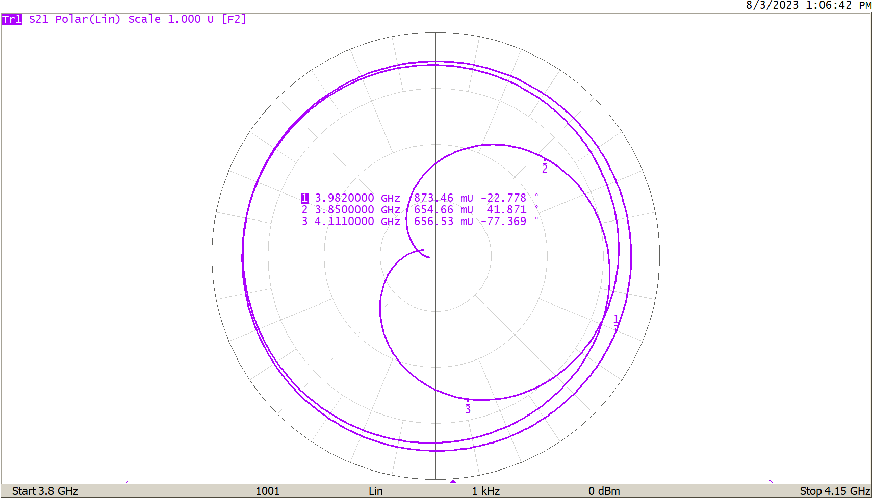
Introduction Fundamentally, a Vector Network Analyzer (VNA) measures RF reflections. In a 50Ω system, reflections occur whenever an impedance other than 50 ohms is encountered by the RF signal. The reflection has a magnitude and a phase with respect to the magnitude and phase of the incident signal and may be characterized as a complex number. The VNA menu allows for a selection of charts which can display complex reflection coefficients in many different ways. Read on to learn more about VNA display formats available for analyzing measurements. Reflection and Reflection Coefficients In optics, if a beam of light traveling in a media with dielectric constant ε1 encounters a region with dielectric constant ε2, there will be a reflection as shown in Figure 1. Figure 1 - Optical Reflection The magnitude of the reflection is related to the difference between the two dielectric constants. The transmitted and reflected waves may be normalized by dividing by the incident wave to arrive at a Reflection Coefficient, Γ. For instance, in the absence of loss, the coefficient for reflection might be 0.2, thus the coefficient for transmission must be 0.8. Here, the reflection coefficient is ratio-metric, and the magnitude of the incident signal is irrelevant. Similarly, an RF voltage wave travelling on a 50Ω transmission line may encounter an impedance other than 50 ohms. This results in a reflection. Specifically, that reflection is given by: Where Z is the encountered impedance. If Z is a complex impedance –which can be expressed as R+jX– such as a resistor and capacitor in series, the reflection coefficient Γ will also be complex. We can choose to display the complex reflection coefficient in the following ways: VNA Display Formats Log Magnitude In this format, the magnitude of the complex reflection coefficient is calculated, the base 10 logarithm is applied, and the result multiplied by 20. The multiplication by 20 makes the result proportional to power instead of voltage. Where the complex reflection coefficient Γ is a+jb. This format is convenient to examine a reflection coefficient over a very wide dynamic range. Details of the low loss in the passband of a filter along with a very deep stopband can be clearly seen in Figure 2. This would not be possible using a linear scale. Figure 2 - Filter Plot Linear Magnitude The linear scale is convenient to examine a transmission coefficient such as S21, where the linear magnitude covers a range within two to three orders of magnitude. Figure 3 shows the same filter from Figure 2 but in the linear scale. Details at markers 2 and 3 are not distinguishable in this format. Figure 3 - Filter in Linear Scale Delay The delay format shows the group delay, which is calculated from -dФ/dω of S21. Ф is the phase of the reflection coefficient and ω is the radian frequency, 2πf. The group delay of the filter in Figure 2 is shown below in Figure 4. Figure 4 - Filter Group Delay VNA Display Format The group delay varies from 7.2 nS to 15.4 nS in the passband of the filter. If a modulated signal were passed through this filter such that some of the modulation bandwidth extends toward the peaks, there would be significant phase distortion (dispersion). Frequencies near the peaks might arrive at the receiver 5 nS or so later than frequencies near the center. Filters can be designed with much flatter delay than this if needed, and this can be evaluated using this delay display mode. Phase The phase of the reflection coefficient can be displayed on the VNA screen. The phase is the arctangent of the ratio of the imaginary and real parts of the coefficient, but it represents the phase alignment of the reflected or transmitted signal with respect to the incident signal. If the two signals are in perfect alignment, the phase difference is zero. The phase depends greatly on the delay experienced by the signal. Figure 5 shows the phase of the signal passed through the filter of Figure 2. Figure 5 - Filter S21 Phase The phase wraps at -180 and 180 degrees. The curvature on the left and right sides is due to the delay variation shown in Figure 4, whereas the phase is reasonably linear where the delay is flat in the middle of the passband. Extended Phase The phase is not wrapped in extended phase mode. The phase will be near zero at low frequencies and then become more and more negative at higher frequencies. The phase will change at a greater rate as more delay is experienced. Figure 6 - Extended Phase Display SWR The Standing Wave Ratio is used on reflection measurements such as S11. Reflections on a transmission line interfere with the incident wave, creating peaks and valleys in the voltage envelope of the RF wave. The ratio of the peaks to the valleys along the transmission line is the SWR. An SWR of 1:1 means there are no peaks or valleys, and hence no reflection. SWR may be calculated from the linear reflection coefficient, Γ. Real and Imag The Real and Imaginary display formats depict the real or the imaginary components of a reflection coefficient. Note, these are not the real and imaginary components of an impedance. If there is no imaginary component, then the impedance contains no reactive component and must be resistive alone. If there is no real component, the impedance must be reactive alone. Polar The polar format plots the complex reflection coefficient within a unit circle with the real component on the horizontal axis and the imaginary component on the vertical axis. This is the most fundamental plot, as it displays the reflection coefficient in its most basic form. All other formats are useful derivations. A reflection coefficient is essentially a complex vector. The polar format plots the magnitude and phase of this vector. A vector is often drawn as an arrow, but a dot at what would be the tip of the vector is drawn to reduce clutter when showing vectors for many frequencies. A VNA display format of a polar chart will have circles of magnitude and radial lines of angle, as shown below in Figure 7. Magnitude is shown in linear format here. Figure 7 - Polar Plot If Polar(log) is chosen, the magnitudes of the makers will be stated in dB format. The polar Smith formats, Smith(log), Smith(Lin), Smith(Re/Im), and Smith(R+jX) are Polar plots with a Smith chart overlay. The Smith overlay maps the polar reflection coefficient to the corresponding impedance, which gives rise to it as calculated from Eq. 1. The variations above merely change the values given by the markers. Figure 8 - Smith(R+jX) Format Smith(log) will give the log magnitude and angle of the reflection. Smith(Lin) will give the linear magnitude and angle. Smith(Re/Im) will give the linear Cartesian format reflection. Smith(R+jX) will give the complex impedance at each point. Smith(G+jB) uses the admittance overlay on the polar plot. Instead of an R+jX impedance, the marker value will show the G+jB admittance, which gives rise to the reflection, where the R+jX mode gives the impedance of a pair of series components, a resistance and a reactance. The equivalent inductance or capacitance at that frequency is also given. The G+jB admittance gives the conductance (inverse of resistance) and the susceptance of two components in parallel. The Smith(R+jX) is convenient for analyzing an impedance, which is best modeled as a series impedance, while Smith(G+jB) is best for analyzing a parallel admittance. Conclusion Different display formats are useful for different measurements. This application note covers several different display formats and their uses. For example, the Log Mag format might be best for evaluating a filter, but the SWR will likely be used to evaluate the input match of an antenna, and the Smith(R+jX) is useful for measuring an impedance and perhaps working out a matching network.

Useful Radio Frequency Engineering Formulas and Charts
February 9, 2023
This application note is a collection of essential formulas and charts for Radio Frequency Engineering.

Using a VNA as a Signal Generator
April 19, 2018
A common question from users of Copper Mountain Technologies’ USB-based Vector Network Analyzers is whether the analyzer can be used as a signal source. Users’ motivations for doing so vary, but most commonly the question arises when an additional source is needed in a test setup but is not available. For example, a source might be needed as the LO to a mixer, to check functionality of another test equipment like a power meter or spectrum analyzer, or to produce a reference clock for use elsewhere in a test system. Fortunately, any CMT VNA can readily be used as a signal source. This application note describes the process of configuring a CMT VNA as a signal source, and the expected performance of an analyzer so-configured. This application note is based on the S2 family of instruments’ software; other instruments will follow similar menu structures and procedures.


