

Optimal Fixture Design with End-Launch SMA Connectors
January 12, 2023Introduction
This article is intended to provide guidance for optimal fixture design of a broadband test fixture using end-launch connectors. Much work has already been published on this subject (see references [1], [2], and [3]), thus this paper will merely summarize that work and provide practical guidance.
End-launch SMA or 3.5mm connectors are commonly used to create test boards for various devices. The connectors are attached to the edge of the circuit board, and micro-strip or coplanar waveguide traces are routed from them to the Device Under Test (DUT). Some form of de-embedding can be performed if extraction of DUT-only characteristics is necessary. Copper Mountain Technologies licenses Automatic Fixture Removal (AFR) software for this purpose.
The AFR program de-embeds the fixture using time domain techniques. For best results, the fixture should be characterized to very high frequencies to achieve the best resolution. If the DUT is to be evaluated at lower frequencies – perhaps 2 GHz – it is still important to characterize the fixture to much higher frequencies – perhaps 18 GHz – as long as there are no discontinuities in the return loss or noticeable resonances. The frequency range of the AFR characterization must stop before any resonances, as these impair the de-embedding process.
Best Practices
The first consideration is to determine how best to feed the RF signal to the DUT. The manufacturer of the high frequency DUT should specify a particular layout, which includes a solder pad and a PCB substrate specification. The solder pad will introduce a capacitance to ground, which will vary with its size, the substrate dielectric constant, and the distance the RF ground beneath the pad. The effect of this capacitance must be factored into the RF performance of the DUT, and for the purpose of this paper we’ll assume this has been taken into account.
Avoid abrupt changes in geometry – as shown in Figure 1 – where the transmission line on the PCB interfaces with the DUT input and output pads. Discontinuities like this greatly impair the return loss of the connection and reduce maximum system bandwidth.

Figure 1 – Wide Trace to Small Pad Discontinuity and Tapered Solution
If there is no alternative solution, the transmission line should be tapered up or down to match the width of the DUT pad. Ideally, design the transmission line to be the same width as the DUT I/O pads.
Transmission Line Choice
The transmission line might be microstrip or coplanar waveguide (CPWG) with ground beneath. Use CPWG for the best high frequency performance. The propagation mode in microstrip is much more dispersive than CPWG due to the greater asymmetry of the air and dielectric interface. CPWG has significant E-Fields near the surface due to the grounds on each side, which somewhat ameliorates this asymmetry. All else being equal, CPWG will exhibit broader band performance with better return loss.
Connector Choice
The best choice for an end-launch SMA connector will have a small pin that makes contact to the transmission line. An excessively large pin will have fringing E-Fields, which add localized capacitance and spoil the return loss. A small flat pin is best, as shown in Figure 2. The inner conductor of the SMA connector itself will be considerably larger and will transition to the smaller pin. Choose the substrate thickness such that this inner pin has reasonable clearance to the RF ground plane to prevent shorting out the center conductor, and to prevent the creation of additional capacitance which will impair the return loss as shown in Figure 3.

Figure 2 – SMA Connector with Flat Pin
Some inexpensive SMA connectors are only rated to a few GHz, so check the data sheet for suitability. A standard SMA connector is rated to 12 GHz, while many improved versions work well to 18 GHz. A 3.5mm connector is required to reach 26.5 GHz.
An example of a subpar connector is one that has a shoulder – as shown in Figure 4 – running vertically between the ground flanges, which hold the body of the connector away from the edge of the PCB, leaving an air gap. This misguided feature is likely intended to prevent shorting the connector center pin to the ground layer of a thin substrate, but the result is a dramatic degradation of return loss above 6 GHz. The flat face of the connector must be flush with the side of the PCB for the best results.
![]()
Figure 3 – Clearance between Center Conductor and First Ground Plane, Substrate Material Not Shown for Clarity

Figure 4 – Undesired Shoulder on Connector Face
Substrate Choice
With the transmission line width mostly determined by the DUT I/O and the minimum dielectric layer thickness determined by the need for clearance to the SMA center pin, the substrate material may be chosen and the geometry of the CPWG determined to meet the 50Ω characteristic impedance requirement. According to Southwest Microwave ([3]), a reasonable range of Rogers 4000 series substrate widths is from 8 to 30 mils, with Rogers 4350 being a common choice for its low loss tangent and fire safety characteristics. The invisible top dielectric material in Figure 3 is about 30 mils thick to ensure clearance between the center pin and the first ground layer.
FR4 material may be used as the RF substrate, but there will be significant insertion loss at high frequencies if the transmission lines are very long. Additionally, FR4 dielectric properties are not consistent from batch to batch and certainly not between different raw board vendors. If intending to use FR4 for the dielectric layer, stay with a single raw board manufacturer.
Ground Stitching for CPWG
The top ground layer and the first RF ground layer beneath it must be connected with a row of ground vias on either side of the trace. These vias should be as close to the CPWG gap as is practical, and the distance between the sides of the holes (pitch minus diameter) should be less than a quarter wavelength at the highest frequency of use.
At 20 GHz in Rogers 4350B material, a quarter wavelength is 80 mils. 20 mil holes with 100 mil pitch results in an 80 mil gap. It isn’t necessary to use tiny holes for the stitching, as the gap between the sides of the holes is more important and larger holes provide a more formidable barrier to the RF signal.

Figure 5 – CPWG with Ground Stitching
The design as shown in Figure 5 is technically correct, but it has a serious problem. There will always be some leakage between the via stitching and the top ground planes on each side, which are open on the left and right edges. The leakage will excite a resonance at a frequency where the distance between the vias and the edge of the board is a quarter wavelength. In this case, with Rogers 4350B material, 223 mils is a quarter wavelength at 7.1 GHz, and the board would have an insertion loss dip at that frequency of several dBs.
To mitigate this, add more rows of vias to push any possible resonances high enough in frequency to be out of the picture. This phenomenon is something to watch out for whenever a CPWG trace is run next to a ground area that might resonate.
Optimizing the Transmission Line
Given the thickness of the dielectric core material, the CPWG transmission line is then designed to have the appropriate thickness and side-to-side gap to the top ground plane to give it a 50Ω characteristic impedance. Note that the change in line impedance with respect to the top gap increases greatly as the gap closes in on the trace – around 10 mils or less. This can present a problem as the edge finish of the copper comprising the gap can cause an unexpectedly large variation in the impedance.
For the best results, the trace and grounds should go all the way to the edge of the board without copper pull-back. PCB vendors do not typically like to do this but will usually do so if asked. The width of the trace should be wider than the connector pin to allow for a taper at the end as shown in Figure 5. This taper is necessary to add a localized inductance to counteract the effect of parasitic capacitance at the coaxial to planar interface.
The E-Fields are perfectly radial inside the coaxial part of the connector, but the coaxial environment abruptly ends at the flush end of the connector. Fringing E-fields loop out from the center conductor into the air and terminate back on the body of the connector. These fields are in addition to the ones that exist both around the trace and beneath it, as shown in Figure 6. They create an excess parasitic capacitance and a resulting dip in the characteristic impedance.

Figure 6 – Fringing Fields
The right amount of trace taper can fix the dip in the characteristic impedance but determining the amount of taper is not easy. Full EM analysis can solve this problem, or one can create a circuit board with an array of different tapers to find the optimal solution empirically.
Using the Time Domain Feature on the VNA to Evaluate Impedance vs Distance
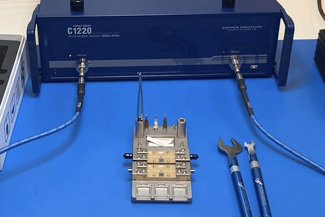
All Vector Network Analyzers (VNAs) sold by Copper Mountain Technologies, except for the M series, have the capability to do advanced time domain analysis. This may be used to evaluate return loss vs position along the trace or, with conversion, characteristic impedance vs position.
To perform this analysis, set the VNA start frequency to its lowest possible frequency and the stop frequency to as high a frequency as the fixture will permit. If the fixture has resonances at high frequencies, the VNA stop frequency must be set at some point below this. Resonances and discontinuities must not be included in the time domain analysis. Set the number of points to the stop frequency divided by the start frequency. In this way, each measured point will be harmonically related. For example, if the start frequency is 1 MHz and the stop is 6000 MHz, set the number of points to 6,000. The measured points will be 1, 2, 3…. 6000 MHz. This arrangement is necessary for the Inverse Fourier Transform (IFFT) to work properly.
Perform a full 2-port calibration on the ends of the test cables, preferably using an Automatic Calibration Module (ACM). Set the VNA to measure a single trace – S11.
Now, navigate to Analysis>Time Domain in the user interface menu. Turn time domain On, then set reflection type to one way. Set the start to -100 pS and the stop to 400 pS or whatever is required to see the effect of the output connector. This should include the coaxial part of the connector starting at 0, and the PCB launch area at 100 pS or so. Set the type to lowpass step as shown in Figure 7.
The Set Frequency Lowpass button will be greyed out, since the start and stop frequencies and number of points have already been set correctly.
Return loss vs time (or distance) will be visible on the VNA screen. To change this to display characteristic impedance, navigate up one level from the time domain menu and select conversion. Set conversion to on and leave the default function Z:Reflection as is.
In the upper left-hand corner of the VNA screen, click on log mag and change it to lin mag. Click on the 0.100 U/ scale and change to 5 (ohms per division). Click on the 0.000 after that and change it to 50 (ohms reference level). You should now see the characteristic impedance vs time on the screen.

Figure 7 – Time Domain Settings
Figure 8 shows the impedance vs distance for an untapered 41 mil trace with 12 mil gap above a 30 mil Rogers 4350B substrate. The lower impedances on each end due to parasitic capacity are clearly visible. The faint line is without taper, and the darker trace has a small taper which improves the impedance change slightly. Optimization of this taper is needed to get even better results, but the return loss in Figure 9 is still better than the 22 dB to 20 GHz in the simulation.
An actual fixture with this sort of return loss performance can be de-embedded using Automatic Fixture Removal with excellent accuracy.

Figure 8 – Characteristic Impedance vs Time

Figure 9 – Return Loss With and Without Taper, Blue line, Grey line
Conclusions
This article describes a logical process for the design of fixturing with good performance to high frequencies. Following these steps should result in fixturing which allows accurate measurement of a DUT, and the ability to de-embed the results using the AFR Software from Copper Mountain Technologies. This article can be used as a resource for those creating RF fixtures; however, CMT does not design fixtures or possess special expertise in this field. Those experts work for companies like Southwest Microwave, SV Microwave, or Fairview Microwave, among others. They will likely assist the designer with the application of their connector products.
Please see the technical documentation on our website www.coppermountaintech.com for more information about time domain techniques, measurement, and calibration, as well as to find information on our many affordable VNA models.
References
[1] Southwest Microwave, Inc., “Optimizing Test Boards for 50 GHz End Launch Connectors”, Web link
[2] Southwest Microwave Inc., “Utilizing Time Domain (TDR) Test Methods for Maximizing Microwave Board Performance”, Web link
[3] Southwest Microwave, Inc., “The Design & Test of Broadband Launches up to 50 GHz on Thin & Thick Substrates”, Web link