High-Speed PCB Design and VNA Testing
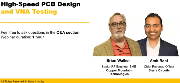
Presented by: Sierra Circuits

Featuring: Brian Walker, Senior RF Engineer SME 


When designing PCBs with operating frequencies beyond 10 GHz, you’ll often encounter challenges such as signal reflections, crosstalk, propagation delay, and EMI. These issues might degrade the S/N ratio and attenuate the transmitted signal. If left unchecked, the signal’s fidelity decreases over time, and the entire system might crash.

In this high-speed PCB webinar, you will learn the key design challenges and techniques to tackle them.


  • What is the OTA Antenna Test System?
  • What applications can it be used for?
  • How to calibrate the VNA for radiation pattern measurement?
  • How to select the correct bundle for your application?
  • Live Measurement Demonstration
High-Speed PCB Design and VNA Testing Webinar

Fill out the following information to receive an email with the link to watch this webinar. Please allow a few minutes for the email to reach your inbox.
By submitting this form, you consent to receiving periodic emails from Copper Mountain Technologies.  Occasionally our responses are considered spam by email management software, so please check your junk folder for emails from any address @coppermountaintech.com or @copper-mountain-technologies.odoo.com. To ensure you always get our emails please whitelist coppermountaintech.com and copper-mountain-technologies.odoo.com domains. All information submitted to Copper Mountain Technologies is for internal purposes only and will not be shared with any third parties. Please visit our Privacy Policy for more information.