

Measurement of Electronic Component Impedance Using A Vector Network Analyzer
March 26, 2019Introduction
Electrical impedance is an important parameter used to describe individual electrical circuit components or a circuit as a whole. Impedance is a complex number, in which the real part is represented by resistance and the imaginary part is represented by reactance. Once the impedance is determined, one can calculate other parameters such as resistance, inductance, capacitance, scattering coefficient, and figure of merit; draw an equivalent circuit of the measured circuit and predict its behavior over the desired frequency band. Several fundamental methods have been developed to measure impedance. Such methods are based on the use of bridges (with or without auto-balancing), resonators, precision current and voltage meters, and network analyzers. The vector network analyzer (VNA) has recently become a powerful tool for analyzing impedance in a broad band, which partially covers the GHz region. One- and two-port circuits for S-parameter measurements allow the user to determine the impedance from milliohms to tens of kilohms using known relationships between the values. The sources of error in such measurements are the analyzer itself and the DUT fixture. In this article, we will describe only those limitations associated with the analyzer, assuming that appropriate de-embedding techniques can minimize the influence of the fixture and thus help to achieve the required measurement stability.
Present-day VNAs perform high-precision S-parameter measurements of one- and multi-port devices. This is achieved through the use of algorithms of VNA precision calibration [1]. Verification methods determining maximum errors in magnitude and phase measurements for transmission and reflection coefficients are available. In VNA uncertainty analysis, apart from maximum error calculation, a covariance matrix based method [2, 3] involving root-mean-square error calculation is widely used. Knowing the probability distribution law of the error, the root-mean-square and maximum values of the error can be related by a coefficient.
Let us consider the impedance and error calculation methods based on the results of S-parameter measurements performed by a vector network analyzer. The method of linearization is the basis for the mathematical tool of the indirect measurement error calculation. All of calculations herein are carried out using the specifications of the precision S5048 Vector Network Analyzer from Copper Mountain Technologies.
Impedance Measurement Configurations
One- and two-port VNAs have recently become widely adopted. One-port analyzers (so-called reflectometers) enable the measurements of a complex reflection coefficient, while two-port instruments measure both a complex reflection coefficient and a complex transmission coefficient.
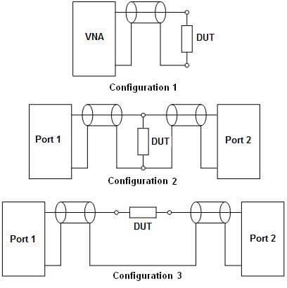
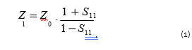
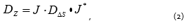
Almost every electrical circuit includes such components as resistors, capacitors, and inductors. Let us consider how one can determine the impedance of a device under test (DUT) having two electric pins. Fig. 1 shows three possible connection configurations of such a DUT. A suitable fixture must be used to connect a DUT to the VNA ports, which normally represent coaxial waveguides of some type. This article does not cover the questions of fixture quality, its influence on the measurement results and the location of a DUT in the fixture.
The first configuration represents reflection coefficient measurement and can be implemented usingeither a reflectometer or a two-port VNA. This configuration is fundamental but has a number of limitations in its application. The second and the third configurations can be implemented only using a two-port VNA as they are aimed at transmission measurements.
Input Impedance Measurement Error
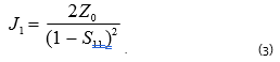
Configuration 1, shown in Fig. 1, measures the reflection coefficient of a load representing a DUT connected between the signal (central) conductor and the screen (outer conductor). The unknown impedance is equal to the load input impedance and represents a complex number. It is known that input impedance can be calculated using the formula:
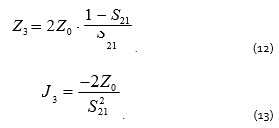
Where Z0 is characteristic impedance of a transmission line (commonly 50 Ohm); S11 is the measured value of the complex reflection coefficient, the subscript indicates the configuration number. The measurement error dispersion of DZ input impedance can be calculated from the known error dispersion DDS of the complex reflection coefficient (or the complex transmission coefficient for configurations 2 and 2) measurement using the linearization method and the formula:
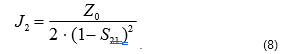
where J is a function derivative with respect to the measured variable (Jacobian); asterisk (*) refers to a complex conjugation operator. To calculate input impedance using formula (1), the analytic form of the derivative with respect to S11 will be:
When describing a VNA, maximum measurement error for the reflection coefficient magnitude is normally specified. This error also defines maximum phase error [4]. It should be taken into account that the mazimum magnitude error of the reflection coefficient (or transmission coefficient) depends on the measured S-parameter. Error dispersion for a complex reflection coefficient can be calculated based on using the formula:
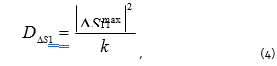
where k is a scaling factor, equal to 3 in the case of uniform measurement error distribution, and equal to 9 in the case of uniform Gaussian distribution. Theoretically, there is no such notion as maximum deviation from the mean in the Gaussian distribution. In practice, however, assuming k is equal to 9, the formula (4) gives the maximum error not greater than the specified error with a probability of 0.99. Further, substituting (4) and (3) into (2), one will get the error dispersion for the input impedance:
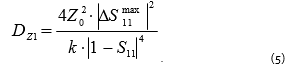
State-of-the-art analyzers feature small measurement error of complex reflection coefficient; that is why dispersion of real and imaginary parts is equal and amounts to half of the measurement error dispersion for input impedance calculated using formula (5).
Maximum error is calculated using the formula:
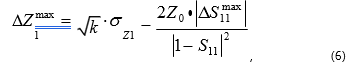
Where δ21=√D21 is the root-mean-square error of the input impedance. Analyzing formulas (5) and (6), one can see that the measurement error dispersion of input impedance and the maximum error will increase significantly when |1-S11| decreases. The complete reflection coefficient close to the value of 1 occurs at certain frequencies for a short circuit load and an open circuit load. Thus, configuration 1 is not applicable for impedance measurements of very low and very high levels. It should also be noted that minimum error is achieved for devices having input impedance |Z1| close to the characteristic impedance of a transmission line.
Low-Level Impedance Measurement
To measure low-level impedance, one should use configuration 2 and measure the transmission coefficient of a two-port THRU, in which the DUT connects the signal conductor and the shield. Only for low impedance DUTs will the transmission coefficient of the THRU will be other than 1. Therefore, fro this case, the DUT impedance can be calculated using the formula:
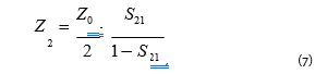
where S21 is the measured value of complex transmission coefficient.
The analytical expression of the derivative with respect to S21, when calculating impedance using formula (7), is as follows:
Using the known effective parameters of a two-port VNA, one can determine the maximum error of the transmission coefficient magnitude . Error dispersion for the transmission coefficient can be calculated in a manner similar to equation (4):
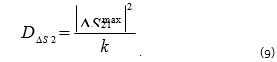
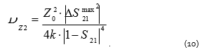
The maximum error in reflection and transmission coefficients of a particular VNA occurs in the case of in-phase summation of several summands [4], which is a highly improbable event. Thus, the assumption of the Gaussian nature of the error (i.e. k 9 ) is much more reasonable in light of the central limit theorem. Further, substituting (9) and (8) into (2), one will get the error dispersion of the impedance:
Maximum error can be calculated using the formula:
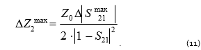
Analyzing formulas (10) and (11), one can see that the measurement error dispersion of impedance and the mazimum error will increase significantly when |1-S21| decreases. If the DUT impedance is low, however, the S21 magnitude will be significantly lower than 1.
Average and High-Level Impedance Measurement
To measure average and high-level impedance, one should use configuration 3 and measure the transmission coefficient of a two-port THRU, in which the DUT is inserted in the signal-conductor gap. If the DUT impedance is high, the THRU transmission coefficient magnitude will be significantly lower than 1. In this case the DUT impedance and its derivative can be calculated using the formulas:
Dispersion is calculated by using the formula (9). To achieve a higher accuracy of calculation, one should take into account that the maximum error of transmission coefficient measurement depends on the transmission coefficient magnitude. Substituting (9) and (13) into (2), one obtains the error dispersion of impedance measurements for configuration 3:
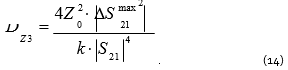
The maximum error can be calculated using the formula:
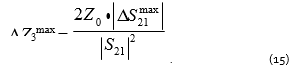
Analyzing formulas (14) and (15), one can see that the measurement error dispersion of impedance and the maximum error will increase significantly when |S21| decreases. When the DUT impedance increases, the S21 magnitude decreases, but the contribution of certain effective parameters of a two-port VNA to overall error of the transmission coefficient decreases as well. Let us consider the relationship between the impedance measurement error and the VNA effective parameters for the case of a particular VNA.
Example of Impedance Maximum Error Calculation and Optimal Configuration Choice
The maximum error of primary measurements can be expressed in terms of effective VNA parameters:
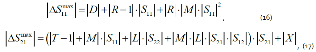
where D is directivity, R is reflection tracking, M is source match, T is transmission tracking, L is load match, and X is isolation. Thus, the maximum measurement error depends on the measured parameter magnitude, i.e. actually on the configuration circuit impedance. Figure 2 shows the calculation results for (6), (11) and (15) with (16) and (17) accounted for. The maximum relative error function of the impedance magnitude is shown on a logarithmic scale. The calculations shown are made using the specifications of the S5048 Vector Network Analyzer from Copper Mountain Technologies [5]. The typical effective parameters of the VNA after full two-port calibration are listed in Table 1. The values were additionally verified using the calibration comparison method [6], for which a precision TRL calibration kit [1] was used.
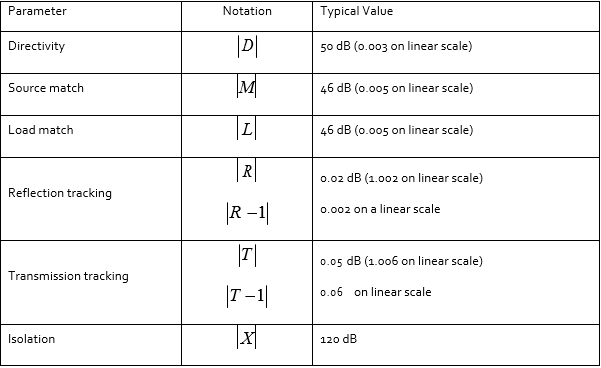
Table 1 – Metrological specifications of S5048 VNA
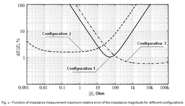
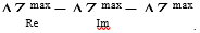
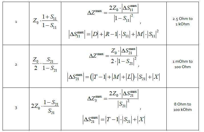
To choose the configuration, one should limit the maximum relative error to a certain level, for example to 10%. Based on this, the summary Table 2 shows the ranges in which the given configurations are most suitable. Table 2 represents basic relations for impedance calculation and expressions showing the relationship between impedance measurement error and effective parameters of the VNA. It should be noted that the specific nature of each configuration is accounted for in the rearrangement of the formulas for calculating maximum error of S- parameters. For a more detailed analysis of the DUT impedance, one can account for maximum errors of the real and imaginary parts determined using the following condition:
Conclusion
Methods of measuring impedance of various levels using a VNA and methods of calculating maximum error have been considered. All the required formulas have been presented. Also, a sample calculation for choosing a measurement configuration using the S5048 VNA has been performed. Under the proposed selection conditions, the impedance measurement error does not exceed 10%.
References
- G. Guba, A.A. Ladur, A.A. Savin, Classificaion and Analysis of Vector Network Analyzer Calibration Methods // Reports of the Tomsk State University of Control Systems and Radioelectronics. – 2011. – no. 2(24), part 1, pp. 149-155.
- F. Williams, A. Lewandowski, P.D. Hale, C.M. Wang, A., Dienstfrey Covariance-Based Vector- Network-Analyzer Uncertainty Analysis for Time- and Frequency-Domain Measurements // IEEE Trans. on Microwave Theory and Techniques, vol. 58, no. 7, pp. 1877-1886, July 2010.
- A. Savin, V.G. Guba, B.D. Maxson, Covariance Based Uncertainty Analysis with Unscented Transformation // 82nd ARFTG Microwave Measurement Conference, Nov. 2013, USA, pp. 15-19.
- A. Savin, V.G. Guba, Determination of Residual Systematic Error After One-Port Calibration // Metrologist’s Bulletin, 2009, no. 4, pp. 16-21.
- Web-site of Copper Mountain Technologies (the USA, Indianapolis) [Electronic source] http://www.coppermountaintech.com/ (free access mode).
- G. Guba, A.A. Savin, O.N. Bykova, A. Rumiantsev, B.D. Maxson, An Automated Method for VNA Accuracy Verification Using the Modified Calibration Comparison Technique // 82nd ARFTG Microwave Measurement Conference, Nov. 2013, USA, pp. 164-167.