

Wi-Fi, Bluetooth & PCB Tuning and Antenna Testing
April 19, 2018Application Profile
Antenna testing is becoming more and more important as the Internet of Things (IoT) starts to materialize. More and more consumer and industrial products are incorporating wireless interfaces such as Bluetooth, WiFi, GPS, or proprietary wireless radio technologies. Adoption of such features has been accelerated by the availability of low cost, integrated modules from a variety of vendors.
Wireless modules are especially beneficial for low- and medium-volume manufacturers for whom the cost of designing a custom solution at the chipset level would never be recovered. For medium and high-volume applications, the additional design and verification cost of adding the chipset to the PCB become more practical and the investment can be recovered by realizing cost savings of chipsets relative to modules. When a custom chipset-based design is pursued, the starting point for layout will usually be a reference design provided by the chipset’s manufacturer.
Modules and reference designs alike will typically specify one or more particular antennas and its match as determined by the vendor. However, this ideal match is nominally determined in an ideal or “typical” environment, most often without any materials nearby which might detune the antenna, reducing its effectiveness and ultimately the range and/or reliability of the wireless interface. When the module includes an antenna on-board, only the module location and surrounding materials can be adjusted to optimize the antenna match. But when a module with external antenna or reference design is adopted, it is possible to optimize the antenna’s performance in the product’s actual housing and including the effects of the PCB itself.
Using a 1-Port VNA, aka vector reflectometer, is one approach to measure and optimize the quality of an antenna and antenna matching network. The measurement result of a one-port VNA is called S11 (read as “Ess One One”) and it measures the signal reflected back to the instrument port relative to the signal transmitted into the device-under-test (DUT). The Copper Mountain Technologies R54 and R140 vector reflectometers are ideally suited for this task, measuring S11 at frequencies up to 5.4 GHz and 14.0 GHz, respectively.
In this application note, we will explain the S11 measurement at an introductory level, talk about some of the specific tools and techniques which will be useful when measuring and optimizing wireless antennas and their matching networks.
S11 (Return Loss) Measurement
Reflectometers, or 1-port VNAs, possess exactly one RF measurement port. The device-under-test (DUT) is connected to this port, either directly or more often, via a combination of cables and adaptors collectively referred to as the fixture. Once connected, we can use the VNA software to configure a set of frequencies to be sequentially tested, and to view the DUT’s measured response on the PC’s graphical user interface.
Just what is being measured? First, let’s consider just a single frequency point. Suppose the VNA outputs an 85 MHz sinusoid tone, from its port. Since there’s only one port on the reflectometer, there’s only one thing to measure, and that’s how much of the generated signal is reflected to, or returned, to the same connector interface, and that’s S11. In general, the signal returned will have a magnitude corresponding to some loss in the fixture and device under test (thus, Return Loss) and will have a phase as well, corresponding to the delay of the device under test at 85 MHz. So although we’re measuring one parameter (S11), it has two components; that’s what makes S11 a “vector” measurement.
In this description, 85 MHz was chosen arbitrarily; the response of the DUT can be measured at any frequency within the VNA’s frequency range. In fact, normally the VNA will be configured to test a number of different frequencies in this same manner. S11 will have some number of Points then, starting at the lowest frequency we test (a Start Frequency), and ending at the highest (a Stop Frequency). We can now plot the magnitude of S11 versus frequency, or the phase of S11 versus frequency. Here is an example of how the magnitude and phase plots may appear.
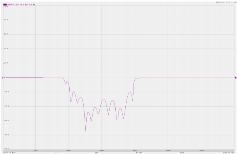
Figure 1: Magnitude vs frequency
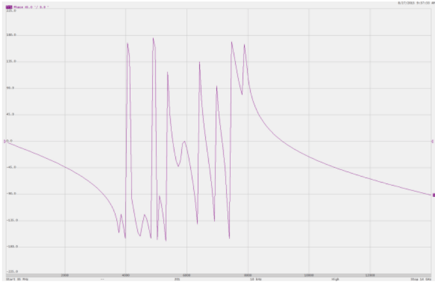
Figure 2: Phase vs frequency
Generally speaking, magnitude return loss (S11) is the more important result of the two. In particular, if we happen to know that our device is an antenna, the magnitude of S11 is the power reflected back to the RF connector—power which is not being radiated by the antenna. So the magnitude of S11 relates inversely to the efficiency of the antenna. S11’s magnitude is usually measured in dB, relative to the signal level transmitted into the DUT.
If the device has zero impedance at its input, or is a “Short”, no voltage can develop at its input terminals and therefore no power can be transferred into the device; all the transmitted power will be reflected back to the signal source. Likewise, if the device has infinite impedance at its input, or is an “Open”, no current can be delivered, and all power will be reflected. Most real-world devices fall somewhere in between, and hopefully somewhere nearer the characteristic impedance of the source (50 Ω, nominally) as this is the impedance at which maximum power is transferred into the device. The closer the device impedance is to the source impedance, the less power is reflected back, and the more is delivered to the device. In the case of an antenna, power sent from the source will either be reflected from or emitted by the antenna. Therefore, S11 return loss is a key performance criterion for any antenna.
As a refresher or for your convenience, the relationship between dB return loss and % power are shown in Table 1, with some commentary relevant to the application of measuring an antenna’s match.
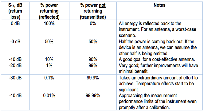
Figure 2: Phase vs frequency
Application Profile
In a real system, we can obviously choose to measure S11 at any of many points in the system. If the antenna being tested has an RF connector where we can connect a test instrument, it’s possible to simply connect the VNA test port to that of the antenna itself using adaptors and cables. In the nomenclature of Wi-Fi or Bluetooth modules, such an antenna may be referred to as an “External” antenna, and may have an SMA or U.FL connector at its input. Antenna testing here is a good starting point, because if S11 of the antenna itself is not working well—it is not transmitting a decent portion of the power you sent to it—you’ll have an uphill battle design-wise to improve its performance.
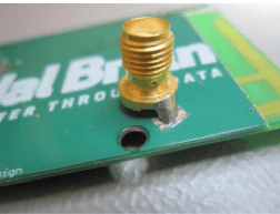
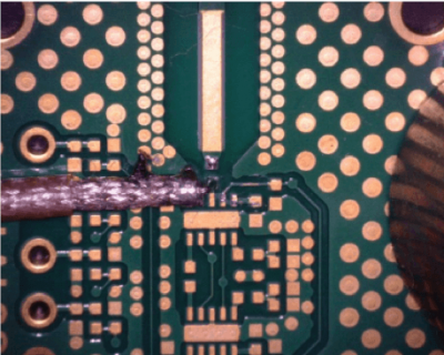
If the antenna itself has a reasonable return loss performance, radiating perhaps 90% or more of the power sent to it, or if it’s an “internal” or chip antenna which can’t be measured directly, a next suitable test will be to measure S11 from a test point on the PCB itself. Generally speaking, there are two ways to accomplish such a measurement. The first is to install an RF connector directly at the point to be tested, as shown in the first figure below. S11 is then measured from this connector.

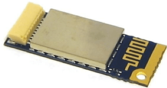
A second approach is to install a connectorized test cable—typically semi-rigid coax—with the signal pin soldered to the test point and shield of the test cable soldered to ground on the PCB. The technique is shown in the figure at right.
The calibration for this case becomes a little tricky because it’s not practical to replace the DUT (the PCB) with a precision Short, Open and Load standard. In this case, an advanced calibration method called port extension is used instead. For more information about Port Extension, refer to the instrument’s operating manual or our application note Calibration Notes and Tips. Once calibration is accomplished at the PCB interface, we can now “see what the chip sees” in the sense that the impedance measured by the VNA corresponds to the impedance into which our wireless chipset must operate. We can now proceed with selecting one or more matching component values to achieve maximal power transfer into the antenna (and minimum return loss) at one or more frequencies of interest for our application.
Conclusion
Increasingly, engineers who have not worked much with RF test and measurement equipment and techniques are in need of tools to optimize the wireless circuits and antennas being added into products. The one-port VNA is an ideal tool for measurement and optimization of such circuits but requires some understanding of calibration and return loss concepts as well as practical steps to take when measuring such a system. With the information in this application note, an engineer with a 1-Port vector reflectometer can begin taking measurements and improving antenna matching circuits.
If you have additional questions about antenna testing or optimization, please contact our support team at support@coppermountaintech.com and we will be glad to help you out.